ZHCSMX7A August 2021 – December 2021 TPS92519-Q1
PRODUCTION DATA
- 1 特性
- 2 应用
- 3 说明
- 4 Revision History
- 5 Pin Configuration and Functions
- 6 Specifications
-
7 Detailed Description
- 7.1 Overview
- 7.2 Functional Block Diagram
- 7.3
Feature Description
- 7.3.1 Buck Converter Switching Operation
- 7.3.2 Switching Frequency and Adaptive On-Time Control
- 7.3.3 Minimum On-Time, Off-Time, and Inductor Ripple
- 7.3.4 Enable
- 7.3.5 LED Current Regulation and Error Amplifier
- 7.3.6 Start-up Sequence
- 7.3.7 Analog Dimming and Forced Continuous Conduction Mode
- 7.3.8 External PWM Dimming and Input Undervoltage Lockout (UVLO)
- 7.3.9 Shunt FET Dimming or Matrix Beam Application
- 7.3.10 Bias Supply
- 7.3.11 Bootstrap Supply
- 7.3.12 Faults and Diagnostics
- 7.3.13 Output Short Circuit Fault
- 7.3.14 Output Open Circuit Fault
- 7.3.15 Parallel Operation
- 7.4 Device Functional Modes
-
8 Application and Implementation
- 8.1
Application Information
- 8.1.1 Duty Cycle Consideration
- 8.1.2 Switching Frequency Selection
- 8.1.3 LED Current Set Point
- 8.1.4 Inductor Selection
- 8.1.5 Output Capacitor Selection
- 8.1.6 Input Capacitor Selection
- 8.1.7 Bootstrap Capacitor Selection
- 8.1.8 Compensation Capacitor Selection
- 8.1.9 Input Undervoltage Protection
- 8.1.10 CSN Protection Diode
- 8.2
Typical Application
- 8.2.1 Design Requirements
- 8.2.2
Detailed Design Procedure
- 8.2.2.1 Calculating Duty Cycle
- 8.2.2.2 Calculating Minimum On-Time and Off-Time
- 8.2.2.3 Minimum Switching Frequency
- 8.2.2.4 LED Current Set Point
- 8.2.2.5 Inductor Selection
- 8.2.2.6 Output Capacitor Selection
- 8.2.2.7 Bootstrap Capacitor Selection
- 8.2.2.8 Compensation Capacitor Selection
- 8.2.2.9 PWM Dimming and Input Voltage Protection
- 8.2.3 Application Curves
- 8.1
Application Information
- 9 Power Supply Recommendations
- 10Layout
- 11Device and Documentation Support
- 12Mechanical, Packaging, and Orderable Information
7.3.8 External PWM Dimming and Input Undervoltage Lockout (UVLO)
The UDIM pin is a multi-function input that features an accurate input voltage detection based on bandgap thresholds with programmable hysteresis as shown in Figure 7-4. This pin functions as the external PWM dimming input for the LEDs and monitors VIN to detect dropout and undervoltage conditions. When the rising pin voltage exceeds the 2.45-V threshold, 10 µA (typical) of current is driven out of the UDIM pin into the resistor divider providing programmable hysteresis. TI recommends a bypass capacitor value of 1 nF between the UDIMx pin and GND to improve noise immunity.
 Figure 7-4 External PWM Dimming
The brightness of LEDs can be varied by modulating the duty cycle of the signal directly connected to the UDIM input. In addition, either an n-channel MOSFET or a Schottky diode can be used to couple an external PWM signal when using UDIM input in conjunction with UVLO functionality. With an n-channel MOSFET, the brightness is proportional to the negative duty cycle of the external PWM signal. With a Schottky diode, the brightness is proportional to the positive duty cycle of the external PWM signal.
Dropout and input undervoltage protection is achieved by connecting the resistor divider network from VIN to UDIM pin and UDIM pin to GND. Dropout protection is activated when UDIM pin voltage drops below VUDIMx(DO, FALLING) threshold but is held above VUDIMx(EN) threshold. In dropout protection mode, the device disables the error amplidier and disconnects the COMP pin to maintain charge on the compensation network. The device continues switching, ensuring fast response with minimum LED current overshoot as the converter recovers from dropout condition. The minimum input voltage, below which dropout protection is activated is programmed using Equation 9.
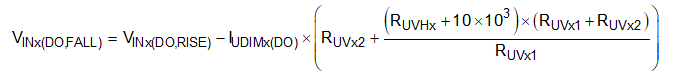
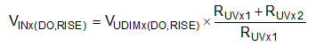
Equation 10 shows the input voltage rising threshold. When VIN exceeds the rising threshold, the error amplifier is enabled and COMP pin is connected to compensation network to regulate LED current.
Additional hysteresis to internal 100 mV is programmed by connecting an extra resistor, RUVHx, in series with UDIM pin. This connection allows the standard resistor divider to have smaller values, minimizing PWM delays.
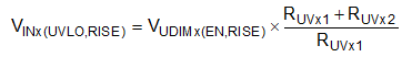
Input undervoltage protection is triggered when UDIM pin voltage drops below VUDIMx(EN) threshold. The device responds to very low VIN voltage or to the external PWM input signal by disabling the error amplifier, disconnecting the COMP pin and tri-stating the switch node. With switching disabled, inductor current and the LED current drop to zero and the charge on the compensation network is maintained. On rising edge of PWM or when VIN exceeds the internal hystersis of 200 mV, the converter resumes switching operation ramping inductor current to the previous steady-state value.
Equation 11 defines the VIN UVLO rising threshold.
Use Equation 12 to determine the VIN UVLO falling threshold.
