ZHCSCA8A March 2014 – April 2019 TPS65286
PRODUCTION DATA.
- 1 特性
- 2 应用
- 3 说明
- 4 Pin Configuration and Functions
- 5 Specifications
-
6 Detailed Description
- 6.1 Overview
- 6.2 Functional Block Diagram
- 6.3
Feature Description
- 6.3.1 Power Switch
- 6.3.2
Buck DCDC Converter
- 6.3.2.1 Output Voltage
- 6.3.2.2 Clock Synchronization
- 6.3.2.3 Error Amplifier
- 6.3.2.4 Slope Compensation
- 6.3.2.5 Enable and Adjusting Under-Voltage Lockout
- 6.3.2.6 Soft-Start Time
- 6.3.2.7 Internal V7V Regulator
- 6.3.2.8 Hard Short Circuit Protection
- 6.3.2.9 Bootstrap Voltage (BST) and Low Dropout Operation
- 6.3.2.10 Thermal Performance
- 6.3.2.11 Loop Compensation
- 6.4 Device Functional Modes
-
7 Application and Implementation
- 7.1 Application Information
- 7.2
Typical Applications
- 7.2.1 Design Requirements
- 7.2.2
Detailed Design Procedure
- 7.2.2.1 Step by Step Design Procedure
- 7.2.2.2 Related Parts
- 7.2.2.3 Inductor Selection
- 7.2.2.4 Output Capacitor Selection
- 7.2.2.5 Input Capacitor Selection
- 7.2.2.6 Soft-Start Capacitor Selection
- 7.2.2.7 Minimum Output Voltage
- 7.2.2.8 Compensation Component Selection
- 7.2.2.9 Auto-Retry Functionality of USB Switches
- 7.2.3 Application Performance Plots
- 8 Power Supply Recommendations
- 9 Layout
- 10器件和文档支持
- 11机械、封装和可订购信息
8 Power Supply Recommendations
The total power dissipation inside TPS65286 should not to exceed the maximum allowable junction temperature of 125°C. The maximum allowable power dissipation is a function of the thermal resistance of the package (θJA) and ambient temperature. The analysis below gives an approximation in calculating junction temperature based on the power dissipation in the package. However, it is important to note that thermal analysis is strongly dependent on additional system level factors. Such factors include air flow, board layout, copper thickness and surface area, and proximity to other devices dissipating power. Good thermal design practice must include all system level factors in addition to individual component analysis.
To calculate the temperature inside the device under continuous load, use the following procedure.
- Define the total continuous current through buck converter (including the load current through power switches). Make sure the continuous current does not exceed maximum load current requirement.
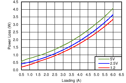
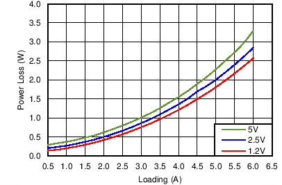
- From the graphs below, determine the expected losses (Y axis) in watts for buck converter inside the device. The loss PD_BUCK depends on the input supply and the selected switching frequency.
- Determine the load current IOUT1 and IOUT2 through the power switches. Read RDS(on)1/2 of power switch from the typical characteristics graph.
- The power loss through power switches can be calculated by PD_PW = RDS1(on) × IOUT1 + RDS2(on) × IOUT2.
- The Dissipating Rating Table provides the thermal resistance θJA for specific packages and board layouts.
- To calculate the maximum temperature inside the IC, use the following formula.
where:
TA = Ambient temperature (°C)
θJA = Thermal resistance (°C/W)
PD_BUCK = Total power dissipation in buck converter (W)
PD_PW = Total power dissipation in power switches (W)
 Figure 58. Power Dissipation of TPS65286,
VIN = 24 V
 Figure 60. Thermal Signature of TPS65286EVM,
TA = Room Temperature, VIN = 24 V,
VOUT to VSW_in = 5 V/0 A, ISW_OUT1/2 = 1.2 A
EVM Board: 4-Layer PCB, 1.6 mm Thickness, 2 oz. Copper Thickness, 65-mm x 65-mm Size, 25 Vias at Thermal Pad
 Figure 59. Power Dissipation of TPS65286,
VIN = 12 V
 Figure 61. Thermal Signature of TPS65286EVM,
TA = Room Temperature, VIN = 24 V, VOUT = 5 V/5 A, ISW_OUT1/2 = 0 A
EVM Board: 4-Layer PCB, 1.6 mm Thickness, 2 oz. Copper Thickness, 65-mm x 65-mm Size, 25 Vias at Thermal Pad