ZHCSCA8A March 2014 – April 2019 TPS65286
PRODUCTION DATA.
- 1 特性
- 2 应用
- 3 说明
- 4 Pin Configuration and Functions
- 5 Specifications
-
6 Detailed Description
- 6.1 Overview
- 6.2 Functional Block Diagram
- 6.3
Feature Description
- 6.3.1 Power Switch
- 6.3.2
Buck DCDC Converter
- 6.3.2.1 Output Voltage
- 6.3.2.2 Clock Synchronization
- 6.3.2.3 Error Amplifier
- 6.3.2.4 Slope Compensation
- 6.3.2.5 Enable and Adjusting Under-Voltage Lockout
- 6.3.2.6 Soft-Start Time
- 6.3.2.7 Internal V7V Regulator
- 6.3.2.8 Hard Short Circuit Protection
- 6.3.2.9 Bootstrap Voltage (BST) and Low Dropout Operation
- 6.3.2.10 Thermal Performance
- 6.3.2.11 Loop Compensation
- 6.4 Device Functional Modes
-
7 Application and Implementation
- 7.1 Application Information
- 7.2
Typical Applications
- 7.2.1 Design Requirements
- 7.2.2
Detailed Design Procedure
- 7.2.2.1 Step by Step Design Procedure
- 7.2.2.2 Related Parts
- 7.2.2.3 Inductor Selection
- 7.2.2.4 Output Capacitor Selection
- 7.2.2.5 Input Capacitor Selection
- 7.2.2.6 Soft-Start Capacitor Selection
- 7.2.2.7 Minimum Output Voltage
- 7.2.2.8 Compensation Component Selection
- 7.2.2.9 Auto-Retry Functionality of USB Switches
- 7.2.3 Application Performance Plots
- 8 Power Supply Recommendations
- 9 Layout
- 10器件和文档支持
- 11机械、封装和可订购信息
6.3.1.3 nFAULT1/2 Response
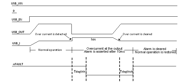
The nFAULT1/nFAULT2 open‐drain output is asserted (active low) during an over current, over temperature or reverse‐voltage condition and remains asserted while the part is latched‐off. The nFAULT signal is de‐asserted once the device power is cycled or the enable is toggled and the device resumes normal operation. The TPS65286 is designed to eliminate false nFAULT reporting by using an internal delay deglitch circuit for over current (10 ms typical) and reverse‐voltage (4 ms typical) conditions without the need for external circuitry. This ensures that nFAULT is not accidentally asserted due to normal operation such as starting into a heavy capacitive load. Deglitching circuitry delays entering and leaving fault conditions. Over temperature conditions are not deglitched and assert the FAULT signal immediately. Figure 22 shows the over current operation of USB switch.
 Figure 22. USB Switch Over Current Operation