ZHCSCA8A March 2014 – April 2019 TPS65286
PRODUCTION DATA.
- 1 特性
- 2 应用
- 3 说明
- 4 Pin Configuration and Functions
- 5 Specifications
-
6 Detailed Description
- 6.1 Overview
- 6.2 Functional Block Diagram
- 6.3
Feature Description
- 6.3.1 Power Switch
- 6.3.2
Buck DCDC Converter
- 6.3.2.1 Output Voltage
- 6.3.2.2 Clock Synchronization
- 6.3.2.3 Error Amplifier
- 6.3.2.4 Slope Compensation
- 6.3.2.5 Enable and Adjusting Under-Voltage Lockout
- 6.3.2.6 Soft-Start Time
- 6.3.2.7 Internal V7V Regulator
- 6.3.2.8 Hard Short Circuit Protection
- 6.3.2.9 Bootstrap Voltage (BST) and Low Dropout Operation
- 6.3.2.10 Thermal Performance
- 6.3.2.11 Loop Compensation
- 6.4 Device Functional Modes
-
7 Application and Implementation
- 7.1 Application Information
- 7.2
Typical Applications
- 7.2.1 Design Requirements
- 7.2.2
Detailed Design Procedure
- 7.2.2.1 Step by Step Design Procedure
- 7.2.2.2 Related Parts
- 7.2.2.3 Inductor Selection
- 7.2.2.4 Output Capacitor Selection
- 7.2.2.5 Input Capacitor Selection
- 7.2.2.6 Soft-Start Capacitor Selection
- 7.2.2.7 Minimum Output Voltage
- 7.2.2.8 Compensation Component Selection
- 7.2.2.9 Auto-Retry Functionality of USB Switches
- 7.2.3 Application Performance Plots
- 8 Power Supply Recommendations
- 9 Layout
- 10器件和文档支持
- 11机械、封装和可订购信息
5.5 Electrical Characteristics
TJ = 25°C, VIN = 24 V, fSW = 500 kHz, RnFAULTx = 100 kΩ (unless otherwise noted)| PARAMETER | TEST CONDITIONS | MIN | TYP | MAX | UNIT | |
|---|---|---|---|---|---|---|
| INPUT SUPPLY | ||||||
| VIN | Input voltage range | VIN1 and VIN2 | 4.5 | 28 | V | |
| IDDSDN | Shutdown supply current | EN1 = EN2 = low | 7.60 | 15 | µA | |
| IDDQ_NSW | Quiescent current without buck switching | EN = high, ENx = low, FB = 1 V
Without buck switching |
0.8 | mA | ||
| IDDQ_SW | Input quiescent current with buck switching | EN = high, ENx = low, FB = 0.6 V
With buck switching |
26 | mA | ||
| UVLO | VIN under voltage lockout | Rising VIN | 4 | 4.25 | 4.50 | V |
| Falling VIN | 3.75 | 4 | 4.25 | |||
| Hysteresis | 0.25 | |||||
| V7V | Low side gate driver, controller, biasing supply | V7V load current = 0 A,
VIN = 24 V |
6.10 | 6.25 | 6.4 | V |
| IOCP_V7V | Current limit of V7V LDO | 83 | mA | |||
| ENABLE | ||||||
| VENR | Enable threshold | Rising | 1.21 | 1.26 | V | |
| VENF | Enable threshold | Falling | 1.10 | 1.17 | V | |
| IENL | Enable pull-up current | EN = 1 V | 3 | µA | ||
| IENH | Enable pull-up current | EN = 1.5 V | 6 | µA | ||
| IENHYS | Enable hysteresis current | 3 | µA | |||
| OSCILLATOR | ||||||
| fSW | Switching frequency | Internal oscillator clock frequency | 400 | 500 | 600 | kHz |
| TSYNC_w | Clock sync minimum pulse width | 80 | ns | |||
| VSYNC_HI | Clock sync high threshold | 2 | V | |||
| VSYNC_LO | Clock sync low threshold | 0.8 | V | |||
| VSYNC_D | Clock falling edge to LX rising edge delay | 120 | ns | |||
| fSYNC | Clock sync frequency range | 200 | 1600 | kHz | ||
| BUCK CONVERTER | ||||||
| VIN | Input supply voltage | 4.5 | 28 | V | ||
| VFB | Feedback voltage | VCOMP = 1.2 V, TJ = 25°C | 0.594 | 0.6 | 0.606 | %/V |
| VCOMP = 1.2 V,
TJ = 40°C to 125°C |
0.588 | 0.6 | 0.612 | |||
| Gm_EA | Error amplifier trans-conductance | -4 µA < ICOMP < 4 µA | 1240 | µS | ||
| Gm_SRC | COMP voltage to inductor current Gm(1) | ILX = 0.5 A | 9.2 | A/V | ||
| ISS | Soft-Start terminal charging current | SS = 1 V | 5.5 | µA | ||
| TSS_INT | Internal Soft-Start time | SS terminal floats | 0.5 | 1 | 1.5 | ms |
| ILIMIT | Buck peak inductor current limit | RLIM = 0 Ω | 6.6 | 7.7 | 8.7 | A |
| RLIM = 200 kΩ | 5.2 | |||||
| TON_MIN | Minimum on time (current sense blanking) | 85 | 120 | ns | ||
| Rdson_HS | On resistance of high side FET | V7V = 6.25 V, includes bondwire resistance | 55 | mΩ | ||
| Rdson_LS | On resistance of low side FET | VIN = 24 V, includes bondwire resistance | 30 | mΩ | ||
| Thiccupwait | Hiccup wait time | 256 | cycles | |||
| Thiccup_re | Hiccup time before re-start | 8192 | cycles | |||
| POWER DISTRIBUTION SWITCH | ||||||
| VSW_IN | Power switch input voltage range | 2.5 | 6 | V | ||
| VUVLO_SW | Input under-voltage lock out | VSW_IN rising | 2.15 | 2.25 | 2.35 | V |
| VSW_IN falling | 2.05 | 2.15 | 2.25 | |||
| Hysteresis | 0.1 | |||||
| RDSON_SW | Power switch NDMOS on-resistance | VSW_INx = 5 V, ISW_OUTx = 0.5 A, TJ = 25°C, includes bondwire resistance | 100 | mΩ | ||
| VSW_INx = 2.5 V, ISW_OUTx = 0.5 A, TJ = 25°C, includes bondwire resistance | 100 | |||||
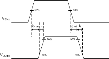
| tD_on | Turn-on delay time | VSW_INx = 5 V, CL = 10 µF,
RL = 100 Ω (see Figure 1) |
1.26 | 1.9 | ms | |
| tD_off | Turn-off delay time | 1.17 | 1.76 | ms | ||
| tr | Output rise time | 0.86 | 1.3 | ms | ||
| tf | Output fall time | 1.37 | 2.06 | ms | ||
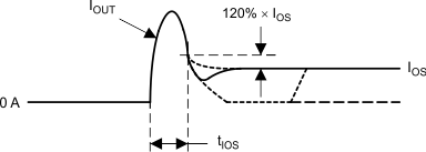
| IOS | Current limit threshold (Maximum DC current delivered to load) and short circuit current, SW_OUT connect to ground | RSET = 14.3 kΩ | 1.65 | 1.76 | 1.87 | A |
| RSET = 20 kΩ | 1.18 | 1.26 | 1.34 | |||
| RSET = 50 kΩ | 0.5 | |||||
| RSET shorted to SW_IN or open | 1.22 | 1.31 | 1.39 | |||
| TIOS | Response time to short circuit | VSW_INx = 5 V | 2 | us | ||
| TDEGLITCH(OCP) | Switch over current fault deglitch | Fault assertion or de-assertion due to over-current condition | 7 | 10 | 13 | ms |
| VL_nFAULT | nFAULTx terminal output low voltage | InFAULTx = 1 mA | 400 | mV | ||
| VEN_SWH | SW_EN1/2 high level input voltage | SW_EN1, SW_EN2 | 2 | V | ||
| VEN_SWL | SW_EN1/2 low level input voltage | SW_EN1, SW_EN2 | 0.4 | V | ||
| RDIS | Discharge resistance(2) | VSW_INx = 5 V, VSW_ENx = 0 V | 104 | Ω | ||
| THERMAL SHUTDOWN | ||||||
| TTRIP_BUCK | Thermal protection trip point | Rising temperature | 160 | °C | ||
| THYST_BUCK | Hysteresis | 20 | °C | |||
| TTRIP_SW | Power switch thermal protection trip point | Rising temperature | 145 | °C | ||
| THYST | Hysteresis | 20 | °C | |||
(1) Ensured by design.
(2) The discharge function is active when the device is disabled (when enable is de-asserted). The discharge function offers a resistive discharge path for the external storage capacitor.
 Figure 1. Power Switches Test Circuit and Voltage Waveforms
  Figure 2. Response Time to Short Circuit Waveform
  Figure 3. Output Voltage vs Current Limit Threshold