ZHCSCA8A March 2014 – April 2019 TPS65286
PRODUCTION DATA.
- 1 特性
- 2 应用
- 3 说明
- 4 Pin Configuration and Functions
- 5 Specifications
-
6 Detailed Description
- 6.1 Overview
- 6.2 Functional Block Diagram
- 6.3
Feature Description
- 6.3.1 Power Switch
- 6.3.2
Buck DCDC Converter
- 6.3.2.1 Output Voltage
- 6.3.2.2 Clock Synchronization
- 6.3.2.3 Error Amplifier
- 6.3.2.4 Slope Compensation
- 6.3.2.5 Enable and Adjusting Under-Voltage Lockout
- 6.3.2.6 Soft-Start Time
- 6.3.2.7 Internal V7V Regulator
- 6.3.2.8 Hard Short Circuit Protection
- 6.3.2.9 Bootstrap Voltage (BST) and Low Dropout Operation
- 6.3.2.10 Thermal Performance
- 6.3.2.11 Loop Compensation
- 6.4 Device Functional Modes
-
7 Application and Implementation
- 7.1 Application Information
- 7.2
Typical Applications
- 7.2.1 Design Requirements
- 7.2.2
Detailed Design Procedure
- 7.2.2.1 Step by Step Design Procedure
- 7.2.2.2 Related Parts
- 7.2.2.3 Inductor Selection
- 7.2.2.4 Output Capacitor Selection
- 7.2.2.5 Input Capacitor Selection
- 7.2.2.6 Soft-Start Capacitor Selection
- 7.2.2.7 Minimum Output Voltage
- 7.2.2.8 Compensation Component Selection
- 7.2.2.9 Auto-Retry Functionality of USB Switches
- 7.2.3 Application Performance Plots
- 8 Power Supply Recommendations
- 9 Layout
- 10器件和文档支持
- 11机械、封装和可订购信息
7.2.3 Application Performance Plots
TA = 25°C, VIN = 24 V, VOUT = 5 V, fSW = 500 kHz, RnFAULT = 100 kΩ (unless otherwise noted)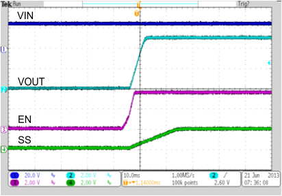 Figure 34. Buck Start Up by EN Terminal With an
External 47-nF SS Capacitor
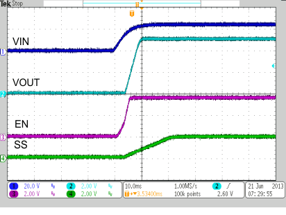 Figure 36. Ramp VIN to Start Up Buck With an
External 22-nF SS Capacitor
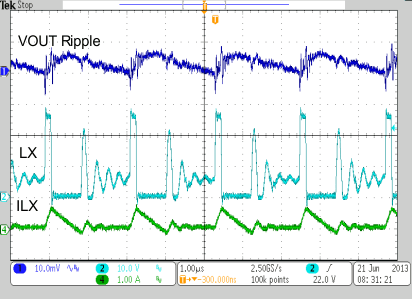 Figure 38. Buck Output Voltage Ripple,
IOUT = 0.1-A PSM Mode
 Figure 40. Buck Output Voltage Ripple, IOUT = 4 A
 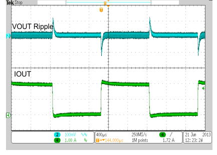 Figure 42. Buck Output Load Transient in PWM Mode,
IOUT = 0 - 2 A
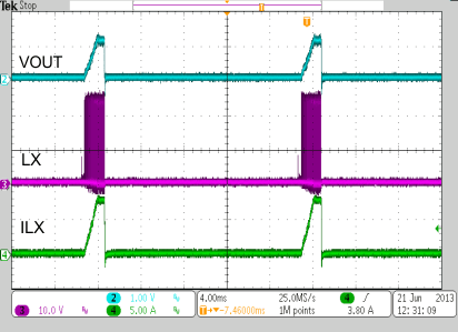 Figure 44. Buck Hiccup Response to Hard Short Circuit
 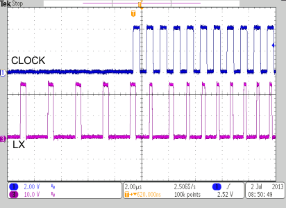 Figure 46. Clock Synchronization Operation
  Figure 48. Power Switch1 Turn on Delay and Rise Time
 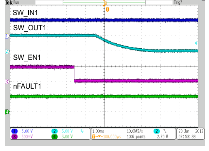 Figure 50. Power Switch1 Turn off Delay and Fall Time, ROUT = 50 Ω, COUT = 10 µF
 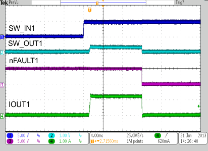 Figure 52. Power Switch1 Enable into Short Circuit
 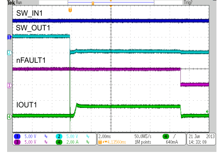 Figure 54. Power Switch1 Current Limit Operation
  Figure 56. Power Switch1 Reverse Voltage Protection Response
  Figure 35. Buck Start Up by EN Terminal With Internal Soft-Start (SS terminal Open)
 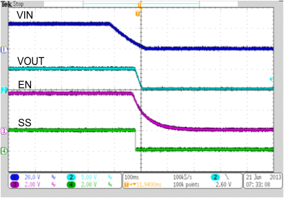 Figure 37. Ramp VIN to Power Down Buck With an
External 22-nF SS Capacitor
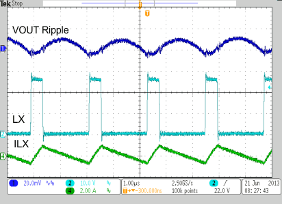 Figure 39. Buck Output Voltage Ripple,
IOUT = 0-A PWM Mode
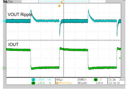 Figure 41. Buck Output Load Transient in PSM Mode,
IOUT = 0 - 2 A
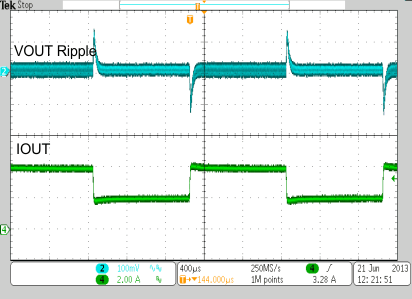 Figure 43. Buck Output Load Transient in PWM Mode,
IOUT = 2 - 4 A
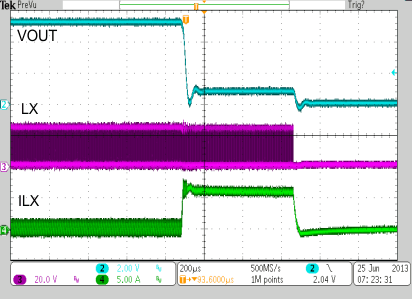 Figure 45. Buck Output Hard Short Response (Zoom In)
 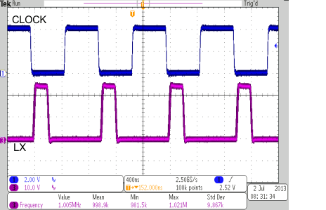 Figure 47. Clock Synchronization at 1 MHz
  Figure 49. Power Switch2 Turn on Delay and Rise Time
 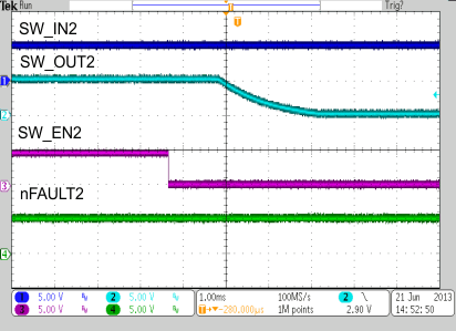 Figure 51. Power Switch2 Turn off Delay and Fall Time, ROUT = 50 Ω, COUT = 10 µF
 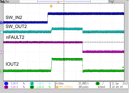 Figure 53. Power Switch2 Enable into Short Circuit
 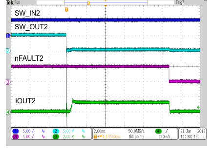 Figure 55. Power Switch2 Current Limit Operation
 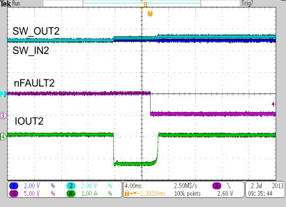 Figure 57. Power Switch2 Reverse Voltage Protection Response