ZHCSCA8A March 2014 – April 2019 TPS65286
PRODUCTION DATA.
- 1 特性
- 2 应用
- 3 说明
- 4 Pin Configuration and Functions
- 5 Specifications
-
6 Detailed Description
- 6.1 Overview
- 6.2 Functional Block Diagram
- 6.3
Feature Description
- 6.3.1 Power Switch
- 6.3.2
Buck DCDC Converter
- 6.3.2.1 Output Voltage
- 6.3.2.2 Clock Synchronization
- 6.3.2.3 Error Amplifier
- 6.3.2.4 Slope Compensation
- 6.3.2.5 Enable and Adjusting Under-Voltage Lockout
- 6.3.2.6 Soft-Start Time
- 6.3.2.7 Internal V7V Regulator
- 6.3.2.8 Hard Short Circuit Protection
- 6.3.2.9 Bootstrap Voltage (BST) and Low Dropout Operation
- 6.3.2.10 Thermal Performance
- 6.3.2.11 Loop Compensation
- 6.4 Device Functional Modes
-
7 Application and Implementation
- 7.1 Application Information
- 7.2
Typical Applications
- 7.2.1 Design Requirements
- 7.2.2
Detailed Design Procedure
- 7.2.2.1 Step by Step Design Procedure
- 7.2.2.2 Related Parts
- 7.2.2.3 Inductor Selection
- 7.2.2.4 Output Capacitor Selection
- 7.2.2.5 Input Capacitor Selection
- 7.2.2.6 Soft-Start Capacitor Selection
- 7.2.2.7 Minimum Output Voltage
- 7.2.2.8 Compensation Component Selection
- 7.2.2.9 Auto-Retry Functionality of USB Switches
- 7.2.3 Application Performance Plots
- 8 Power Supply Recommendations
- 9 Layout
- 10器件和文档支持
- 11机械、封装和可订购信息
6.3.2.8 Hard Short Circuit Protection
The peak inductor current limit trip of buck converter is set by an external resistor at the RLIM terminal. The peak inductor current threshold for over current protection can be calculated by Equation 6.
 Figure 27. Current-Limit Threshold vs RLIM
 The device is protected from over current conditions by cycle-by-cycle current limiting on both the high-side MOSFET and the low-side MOSFET.
High-side MOSFET over current protection:
The device implements current mode control which uses the COMP terminal voltage to control the turn off of the high-side MOSFET and the turn on of the low-side MOSFET on a cycle-by-cycle basis. Each cycle the switch current and the current reference generated by the COMP terminal voltage are compared, the peak switch current intersects the current reference and the high-side switch is turned off.
Low-side MOSFET over current protection:
While the low-side MOSFET is turned on, its conduction current is monitored by the internal circuitry. During normal operation, the low-side MOSFET sources current to the load. At the end of every clock cycle, the low-side MOSFET sourcing current is compared to the internally sourcing current limit threshold. If the low-side sourcing current is exceeded, the high-side MOSFET is turned off and the low-side MOSFET is forced on for the next cycle. The high-side MOSFET is turned on again when the low-side current is below the low-side sourcing current limit threshold at the start of a cycle.
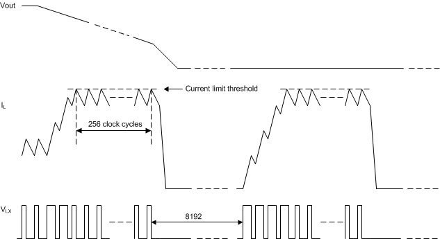
The low-side MOSFET may also sink current from the load. If the low-side sinking current limit is exceeded, the low-side MOSFET is turned off immediately for the rest of that clock cycle. In this scenario both MOSFETs are off until the next cycle. Furthermore, if an output overload condition (as measured by the COMP terminal voltage) has lasted for more than the hiccup wait time which is programmed for 256 switching cycles, the device will shut down and recover after the hiccup time of 8192 cycles. The hiccup mode helps to reduce the device power dissipation under over current conditions.
 Figure 28. DCDC Over-Current Protection