ZHCSCA8A March 2014 – April 2019 TPS65286
PRODUCTION DATA.
- 1 特性
- 2 应用
- 3 说明
- 4 Pin Configuration and Functions
- 5 Specifications
-
6 Detailed Description
- 6.1 Overview
- 6.2 Functional Block Diagram
- 6.3
Feature Description
- 6.3.1 Power Switch
- 6.3.2
Buck DCDC Converter
- 6.3.2.1 Output Voltage
- 6.3.2.2 Clock Synchronization
- 6.3.2.3 Error Amplifier
- 6.3.2.4 Slope Compensation
- 6.3.2.5 Enable and Adjusting Under-Voltage Lockout
- 6.3.2.6 Soft-Start Time
- 6.3.2.7 Internal V7V Regulator
- 6.3.2.8 Hard Short Circuit Protection
- 6.3.2.9 Bootstrap Voltage (BST) and Low Dropout Operation
- 6.3.2.10 Thermal Performance
- 6.3.2.11 Loop Compensation
- 6.4 Device Functional Modes
-
7 Application and Implementation
- 7.1 Application Information
- 7.2
Typical Applications
- 7.2.1 Design Requirements
- 7.2.2
Detailed Design Procedure
- 7.2.2.1 Step by Step Design Procedure
- 7.2.2.2 Related Parts
- 7.2.2.3 Inductor Selection
- 7.2.2.4 Output Capacitor Selection
- 7.2.2.5 Input Capacitor Selection
- 7.2.2.6 Soft-Start Capacitor Selection
- 7.2.2.7 Minimum Output Voltage
- 7.2.2.8 Compensation Component Selection
- 7.2.2.9 Auto-Retry Functionality of USB Switches
- 7.2.3 Application Performance Plots
- 8 Power Supply Recommendations
- 9 Layout
- 10器件和文档支持
- 11机械、封装和可订购信息
6.3.2.11 Loop Compensation
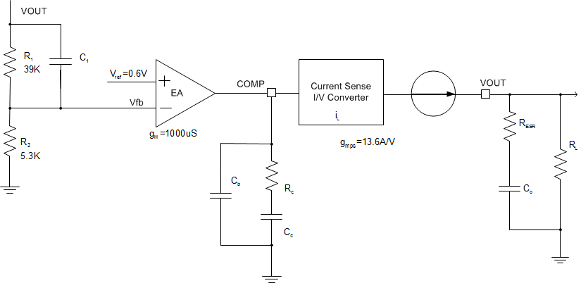
The integrated buck DCDC converter in TPS65286 incorporates a peak current mode. The error amplifier is a trans-conductance amplifier with a gain of 1000 µA/V. A typical type II compensation circuit adequately delivers a phase margin between 60° and 90°. Cb adds a high frequency pole to attenuate high frequency noise when needed. To calculate the external compensation components, follow these steps:
- Select switching frequency, fSW, that is appropriate for application depending on L and C sizes, output ripple, and EMI. Switching frequency between 500 kHz to 1 MHz gives the best trade off between performance and cost. To optimize efficiency, lower switching frequency is desired.
- Set up cross over frequency, fc, which is typically between 1/5 and 1/20 of fSW.
- RC can be determined by:
- Calculate CC by placing a compensation zero at or before the dominant pole (fp = 1 / CO x RL x 2π).
- Optional Cb can be used to cancel the zero from the ESR associated with CO.
- Type III compensation can be implemented with the addition of one capacitor, C1. This allows for slightly higher loop bandwidths and higher phase margins. If used, C1 is calculated from Equation 10.
Equation 7. 

where gM is the error amplifier gain (1000 µA/V), gmps is the power stage voltage to current conversion gain (10 A/V).
Equation 8. 

Equation 9. 

Equation 10. 

 Figure 29. DCDC Loop Compensation