ZHCSCA8A March 2014 – April 2019 TPS65286
PRODUCTION DATA.
- 1 特性
- 2 应用
- 3 说明
- 4 Pin Configuration and Functions
- 5 Specifications
-
6 Detailed Description
- 6.1 Overview
- 6.2 Functional Block Diagram
- 6.3
Feature Description
- 6.3.1 Power Switch
- 6.3.2
Buck DCDC Converter
- 6.3.2.1 Output Voltage
- 6.3.2.2 Clock Synchronization
- 6.3.2.3 Error Amplifier
- 6.3.2.4 Slope Compensation
- 6.3.2.5 Enable and Adjusting Under-Voltage Lockout
- 6.3.2.6 Soft-Start Time
- 6.3.2.7 Internal V7V Regulator
- 6.3.2.8 Hard Short Circuit Protection
- 6.3.2.9 Bootstrap Voltage (BST) and Low Dropout Operation
- 6.3.2.10 Thermal Performance
- 6.3.2.11 Loop Compensation
- 6.4 Device Functional Modes
-
7 Application and Implementation
- 7.1 Application Information
- 7.2
Typical Applications
- 7.2.1 Design Requirements
- 7.2.2
Detailed Design Procedure
- 7.2.2.1 Step by Step Design Procedure
- 7.2.2.2 Related Parts
- 7.2.2.3 Inductor Selection
- 7.2.2.4 Output Capacitor Selection
- 7.2.2.5 Input Capacitor Selection
- 7.2.2.6 Soft-Start Capacitor Selection
- 7.2.2.7 Minimum Output Voltage
- 7.2.2.8 Compensation Component Selection
- 7.2.2.9 Auto-Retry Functionality of USB Switches
- 7.2.3 Application Performance Plots
- 8 Power Supply Recommendations
- 9 Layout
- 10器件和文档支持
- 11机械、封装和可订购信息
7.2.2.9 Auto-Retry Functionality of USB Switches
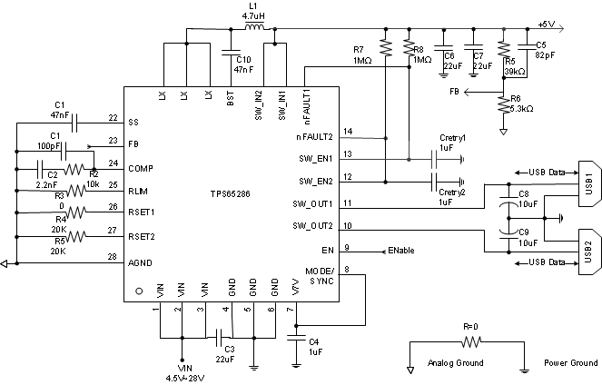
Some applications require that an over-current condition disables the part momentarily during a fault condition and re-enables after a pre-set time. This auto-retry functionality can be implemented with external resistors and capacitor shown in Figure 32. During a fault condition, nFAULT pulls low disabling the part. The part is disabled when EN is pulled low, and nFAULT goes high impedance allowing CRETRY1/2 to be charged. The part re-enables when the voltage on EN_SW reaches the turn-on threshold, and the auto-retry time is determined by the resistor/capacitor time constant. The part will continue to cycle in this manner until the fault condition is removed.
 Figure 32. Auto Retry Functionality
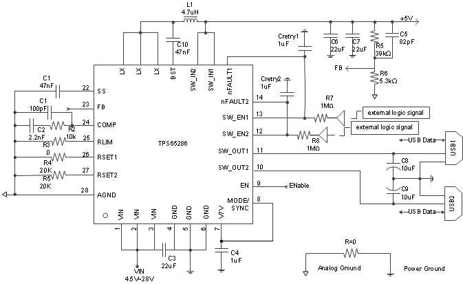
 Some applications require auto-retry functionality and the ability to enable/disable with an external logic signal. Figure 33 shows how an external logic signal can drive EN_SW through RFAULT and maintain auto-retry functionality. The resistor/capacitor time constant determines the auto-retry time-out period.
 Figure 33. Auto Retry Functionality With External Enable Signal