ZHCSO86C December 2022 – August 2025 LM74900-Q1 , LM74910-Q1 , LM74910H-Q1
PRODUCTION DATA
- 1
- 1 特性
- 2 应用
- 3 说明
- 4 器件比较表
- 5 引脚配置和功能
- 6 规格
- 7 参数测量信息
- 8 详细说明
- 9 应用和实施
- 10器件和文档支持
- 11修订历史记录
- 12机械、封装和可订购信息
封装选项
请参考 PDF 数据表获取器件具体的封装图。
机械数据 (封装 | 引脚)
- RGE|24
散热焊盘机械数据 (封装 | 引脚)
- RGE|24
订购信息
9.2.4 MOSFET 选择:阻断 MOSFET Q1
选择阻断 MOSFET Q1 时,重要的电气参数包括最大持续漏极电流 ID、最大漏源电压 VDS(MAX)、最大漏源电压 VGS(MAX)、通过体二极管的最大源极电流以及漏源导通电阻 RDSON。
最大持续漏极电流 ID 额定值必须超过最大持续负载电流。
最大漏源电压 VDS(MAX) 必须足够高,以便承受应用中所见的最高差分电压。这包括所有汽车瞬态事件和任何预期的故障情况。建议使用 VDS 额定电压为 60V 的 MOSFET 以及单个双向 TVS,或使用 VDS 最大额定值为 40V 的 MOSFET 以及两个背对背连接在输入端的单向 TVS。
LM74900-Q1 可驱动的最大 VGS 为 14V,因此应选择 VGS 最小额定值为 15V 的 MOSFET。如果选择了 VGS 额定值小于 15V 的 MOSFET,则可以使用齐纳二极管将 VGS 钳制到安全电平,但这会导致 IQ 电流增加。
为了减少 MOSFET 传导损耗,应尽可能降低 RDS(ON),但根据低 RDS(ON) 选择 MOSFET 可能并非总能如愿。更高的 RDS(ON) 将在更低反向电流级别为 LM74900-Q1 反向比较器提供更高电压信息。随着 RDS(ON) 的增加,反向电流检测效果更好。选择一个在最大电流时正向压降小于 50mV 的 MOSFET 是一个很好的起点。
为了对电池电源电压上的交流叠加纹波进行有源整流,必须选择 Q1 的栅源电荷 QGS 来满足所需的交流纹波频率。每个周期用于有源整流的最大栅源电荷 QGS(在 VGS 等于 4.5V 时)为
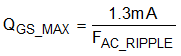
其中 1.3mA 是 VDGATE - VA 为 7V 时的最小电荷泵电流,FAC_RIPPLE 是叠加在电池上的交流纹波的频率,QGS_MAX 是制造商数据表中指定的 6V VGS 时的 QGS 值。对于 FAC_RIPPLE = 30KHz 时的有源整流,QGS_MAX = 43nC。
根据设计要求选择了 BUK7Y4R8-60E MOSFET,其额定值为:
- 60V VDS(MAX) 和 ±20V VGS(MAX)
- RDS(ON) 在 5V VGS 下的典型值为 5.0mΩ,在 10V VGS 下的额定值为 2.9mΩ
- MOSFET QGS 17.4nC
应根据 MOSFET 的预期最大功率耗散来考虑 MOSFET 的热阻,确保结温 (TJ) 得到良好控制。