ZHCSO86C December 2022 – August 2025 LM74900-Q1 , LM74910-Q1 , LM74910H-Q1
PRODUCTION DATA
- 1
- 1 特性
- 2 应用
- 3 说明
- 4 器件比较表
- 5 引脚配置和功能
- 6 规格
- 7 参数测量信息
- 8 详细说明
- 9 应用和实施
- 10器件和文档支持
- 11修订历史记录
- 12机械、封装和可订购信息
封装选项
请参考 PDF 数据表获取器件具体的封装图。
机械数据 (封装 | 引脚)
- RGE|24
散热焊盘机械数据 (封装 | 引脚)
- RGE|24
订购信息
9.4.1 瞬态保护
当外部 MOSFET 在过压切断、反向电流阻断、过流切断、EN 导致电流中断等条件下关断时,输入线路电感会在输入端产生正电压尖峰,而输出电感会在输出端产生负电压尖峰。电压尖峰(瞬变)的峰值振幅取决于与器件输入或输出串联的电感值。如果未采取措施解决此问题,这些瞬变可能会超过器件的绝对最大额定值。
解决瞬变的典型方法包括:
- 最大限度减少进出器件的引线长度和电感。
- 使用较大的 PCB GND 平面。
- 在输出端和 GND 使用肖特基二极管来吸收负尖峰。
- 使用低容值陶瓷电容器(C(IN) 低至约 0.1μF)来吸收能量并抑制瞬变。
输入电容的近似值可通过公式 8 进行估算。
方程式 18. 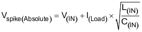
其中
- V(IN) 是标称电源电压
- I(LOAD) 是负载电流
- L(IN) 等于在源极中观察到的有效电感
- C(IN) 是输入端存在的电容
某些应用可能需要额外的瞬态电压抑制器 (TVS),以防止瞬变超过器件的绝对最大额定值。这些瞬变可能会在 EMC 测试(例如汽车 ISO7637 脉冲)期间发生。
 图 9-27 典型应用图