ZHCSOU1 February 2023 DS90UB638-Q1
PRODUCTION DATA
- 1 特性
- 2 应用
- 3 说明
- 4 Revision History
- 5 Pin Configuration and Functions
-
6 Specifications
- 6.1 Absolute Maximum Ratings
- 6.2 ESD Ratings
- 6.3 Recommended Operating Conditions
- 6.4 Thermal Information
- 6.5 DC Electrical Characteristics
- 6.6 AC Electrical Characteristics
- 6.7 AC Electrical Characteristics CSI-2
- 6.8 Recommended Timing for the Serial Control Bus
- 6.9 Timing Diagrams
- 6.10 Typical Characteristics
-
7 Detailed Description
- 7.1 Overview
- 7.2 Functional Block Diagram
- 7.3 Feature Description
- 7.4
Device Functional Modes
- 7.4.1 CSI-2 Mode
- 7.4.2 RAW Mode
- 7.4.3 RX MODE Pin
- 7.4.4 REFCLK
- 7.4.5 Crystal Recommendations
- 7.4.6 Receiver Port Control
- 7.4.7 LOCK and PASS Status
- 7.4.8 Adaptive Equalizer
- 7.4.9 Channel Monitor Loop-Through Output Driver (CMLOUT)
- 7.4.10 RX Port Status
- 7.4.11 Sensor Status
- 7.4.12 GPIO Support
- 7.4.13 Line Valid and Frame Valid Indicators
- 7.4.14 CSI-2 Protocol Layer
- 7.4.15 CSI-2 Short Packet
- 7.4.16 CSI-2 Long Packet
- 7.4.17 CSI-2 Data Type Identifier
- 7.4.18 Virtual Channel and Context
- 7.4.19 CSI-2 Transmitter Frequency
- 7.4.20 CSI-2 Replicate Mode
- 7.4.21 CSI-2 Transmitter Output Control
- 7.4.22 CSI-2 Transmitter Status
- 7.4.23 Video Buffers
- 7.4.24 CSI-2 Line Count and Line Length
- 7.4.25 FrameSync Operation
- 7.5
Programming
- 7.5.1 Serial Control Bus and Bidirectional Control Channel
- 7.5.2 I2C Target Operation
- 7.5.3 Remote Target Operation
- 7.5.4 Remote Target Addressing
- 7.5.5 I2C Controller Proxy
- 7.5.6 I2C Controller Proxy Timing
- 7.5.7 Interrupt Support
- 7.5.8 Error Handling
- 7.5.9 Pattern Generation
- 7.5.10 FPD-Link BIST Mode
- 7.6 Unique ID
- 7.7
Register Maps
- 7.7.1 I2C Device ID Register
- 7.7.2 Reset Register
- 7.7.3 General Configuration Register
- 7.7.4 Revision/Mask ID Register
- 7.7.5 DEVICE_STS Register
- 7.7.6 PAR_ERR_THOLD_HI Register
- 7.7.7 PAR_ERR_THOLD_LO Register
- 7.7.8 BCC Watchdog Control Register
- 7.7.9 I2C Control 1 Register
- 7.7.10 I2C Control 2 Register
- 7.7.11 SCL High Time Register
- 7.7.12 SCL Low Time Register
- 7.7.13 RX_PORT_CTL Register
- 7.7.14 IO_CTL Register
- 7.7.15 GPIO_PIN_STS Register
- 7.7.16 GPIO_INPUT_CTL Register
- 7.7.17 GPIO0_PIN_CTL Register
- 7.7.18 GPIO1_PIN_CTL Register
- 7.7.19 GPIO2_PIN_CTL Register
- 7.7.20 GPIO3_PIN_CTL Register
- 7.7.21 GPIO4_PIN_CTL Register
- 7.7.22 GPIO5_PIN_CTL Register
- 7.7.23 GPIO6_PIN_CTL Register
- 7.7.24 RESERVED Register
- 7.7.25 FS_CTL Register
- 7.7.26 FS_HIGH_TIME_1 Register
- 7.7.27 FS_HIGH_TIME_0 Register
- 7.7.28 FS_LOW_TIME_1 Register
- 7.7.29 FS_LOW_TIME_0 Register
- 7.7.30 MAX_FRM_HI Register
- 7.7.31 MAX_FRM_LO Register
- 7.7.32 CSI_PLL_CTL Register
- 7.7.33 FWD_CTL1 Register
- 7.7.34 FWD_CTL2 Register
- 7.7.35 FWD_STS Register
- 7.7.36 INTERRUPT_CTL Register
- 7.7.37 INTERRUPT_STS Register
- 7.7.38 RESERVED Register
- 7.7.39 CSI_CTL Register
- 7.7.40 CSI_CTL2 Register
- 7.7.41 CSI_STS Register
- 7.7.42 CSI_TX_ICR Register
- 7.7.43 CSI_TX_ISR Register
- 7.7.44 CSI_TEST_CTL Register
- 7.7.45 CSI_TEST_PATT_HI Register
- 7.7.46 CSI_TEST_PATT_LO Register
- 7.7.47 RESERVED Register
- 7.7.48 RESERVED Register
- 7.7.49 RESERVED Register
- 7.7.50 RESERVED Register
- 7.7.51 RESERVED Register
- 7.7.52 RESERVED Register
- 7.7.53 SFILTER_CFG Register
- 7.7.54 AEQ_CTL1 Register
- 7.7.55 AEQ_ERR_THOLD Register
- 7.7.56 RESERVED Register
- 7.7.57 FPD3_CAP Register
- 7.7.58 FPD3_PORT_SEL Register
- 7.7.59 RX_PORT_STS1 Register
- 7.7.60 RX_PORT_STS2 Register
- 7.7.61 RX_FREQ_HIGH Register
- 7.7.62 RX_FREQ_LOW Register
- 7.7.63 SENSOR_STS_0 Register
- 7.7.64 SENSOR_STS_1 Register
- 7.7.65 SENSOR_STS_2 Register
- 7.7.66 SENSOR_STS_3 Register
- 7.7.67 RX_PAR_ERR_HI Register
- 7.7.68 RX_PAR_ERR_LO Register
- 7.7.69 BIST_ERR_COUNT Register
- 7.7.70 BCC_CONFIG Register
- 7.7.71 DATAPATH_CTL1 Register
- 7.7.72 DATAPATH_CTL2 Register
- 7.7.73 SER_ID Register
- 7.7.74 SER_ALIAS_ID Register
- 7.7.75 TargetID[0] Register
- 7.7.76 TargetID[1] Register
- 7.7.77 TargetID[2] Register
- 7.7.78 TargetID[3] Register
- 7.7.79 TargetID[4] Register
- 7.7.80 TargetID[5] Register
- 7.7.81 TargetID[6] Register
- 7.7.82 TargetID[7] Register
- 7.7.83 TargetAlias[0] Register
- 7.7.84 TargetAlias[1] Register
- 7.7.85 TargetAlias[2] Register
- 7.7.86 TargetAlias[3] Register
- 7.7.87 TargetAlias[4] Register
- 7.7.88 TargetAlias[5] Register
- 7.7.89 TargetAlias[6] Register
- 7.7.90 TargetAlias[7] Register
- 7.7.91 PORT_CONFIG Register
- 7.7.92 BC_GPIO_CTL0 Register
- 7.7.93 BC_GPIO_CTL1 Register
- 7.7.94 CSI_VC_MAP Register
- 7.7.95 LINE_COUNT_HI Register
- 7.7.96 LINE_COUNT_LO Register
- 7.7.97 LINE_LEN_1 Register
- 7.7.98 LINE_LEN_0 Register
- 7.7.99 FREQ_DET_CTL Register
- 7.7.100 MAILBOX_1 Register
- 7.7.101 MAILBOX_2 Register
- 7.7.102 CSI_RX_STS Register
- 7.7.103 CSI_ERR_COUNTER Register
- 7.7.104 PORT_CONFIG2 Register
- 7.7.105 PORT_PASS_CTL Register
- 7.7.106 SEN_INT_RISE_CTL Register
- 7.7.107 SEN_INT_FALL_CTL Register
- 7.7.108 RESERVED Register
- 7.7.109 REFCLK_FREQ Register
- 7.7.110 RESERVED Register
- 7.7.111 IND_ACC_CTL Register
- 7.7.112 IND_ACC_ADDR Register
- 7.7.113 IND_ACC_DATA Register
- 7.7.114 BIST Control Register
- 7.7.115 RESERVED Register
- 7.7.116 RESERVED Register
- 7.7.117 RESERVED Register
- 7.7.118 RESERVED Register
- 7.7.119 MODE_IDX_STS Register
- 7.7.120 LINK_ERROR_COUNT Register
- 7.7.121 FPD3_ENC_CTL Register
- 7.7.122 RESERVED Register
- 7.7.123 GPIO_PD_CTL Register
- 7.7.124 PORT_DEBUG Register
- 7.7.125 AEQ_CTL2 Register
- 7.7.126 AEQ_STATUS Register
- 7.7.127 ADAPTIVE EQ BYPASS Register
- 7.7.128 AEQ_MIN_MAX Register
- 7.7.129 RESERVED Register
- 7.7.130 RESERVED Register
- 7.7.131 PORT_ICR_HI Register
- 7.7.132 PORT_ICR_LO Register
- 7.7.133 PORT_ISR_HI Register
- 7.7.134 PORT_ISR_LO Register
- 7.7.135 FC_GPIO_STS Register
- 7.7.136 FC_GPIO_ICR Register
- 7.7.137 SEN_INT_RISE_STS Register
- 7.7.138 SEN_INT_FALL_STS Register
- 7.7.139 FPD3_RX_ID0 Register
- 7.7.140 FPD3_RX_ID1 Register
- 7.7.141 FPD3_RX_ID2 Register
- 7.7.142 FPD3_RX_ID3 Register
- 7.7.143 FPD3_RX_ID4 Register
- 7.7.144 FPD3_RX_ID5 Register
- 7.7.145 I2C_RX0_ID Register
- 7.7.146 RESERVED Register
- 7.7.147 RESERVED Register
- 7.7.148 Indirect Access Registers
- 7.7.149 249
- 7.7.150 Reserved Register
- 7.7.151 PGEN_CTL Register
- 7.7.152 PGEN_CFG Register
- 7.7.153 PGEN_CSI_DI Register
- 7.7.154 PGEN_LINE_SIZE1 Register
- 7.7.155 PGEN_LINE_SIZE0 Register
- 7.7.156 PGEN_BAR_SIZE1 Register
- 7.7.157 PGEN_BAR_SIZE0 Register
- 7.7.158 PGEN_ACT_LPF1 Register
- 7.7.159 PGEN_ACT_LPF0 Register
- 7.7.160 PGEN_TOT_LPF1 Register
- 7.7.161 PGEN_TOT_LPF0 Register
- 7.7.162 PGEN_LINE_PD1 Register
- 7.7.163 PGEN_LINE_PD0 Register
- 7.7.164 PGEN_VBP Register
- 7.7.165 PGEN_VFP Register
- 7.7.166 PGEN_COLOR0 Register
- 7.7.167 PGEN_COLOR1 Register
- 7.7.168 PGEN_COLOR2 Register
- 7.7.169 PGEN_COLOR3 Register
- 7.7.170 PGEN_COLOR4 Register
- 7.7.171 PGEN_COLOR5 Register
- 7.7.172 PGEN_COLOR6 Register
- 7.7.173 PGEN_COLOR7 Register
- 7.7.174 PGEN_COLOR8 Register
- 7.7.175 PGEN_COLOR9 Register
- 7.7.176 PGEN_COLOR10 Register
- 7.7.177 PGEN_COLOR11 Register
- 7.7.178 PGEN_COLOR12 Register
- 7.7.179 PGEN_COLOR13 Register
- 7.7.180 PGEN_COLOR14 Register
- 7.7.181 RESERVED Register
- 7.7.182 CSI0_TCK_PREP Register
- 7.7.183 CSI0_TCK_ZERO Register
- 7.7.184 CSI0_TCK_TRAIL Register
- 7.7.185 CSI0_TCK_POST Register
- 7.7.186 CSI0_THS_PREP Register
- 7.7.187 CSI0_THS_ZERO Register
- 7.7.188 CSI0_THS_TRAIL Register
- 7.7.189 CSI0_THS_EXIT Register
- 7.7.190 CSI0_TPLX Register
- 7.7.191 291
- 8 Application and Implementation
- 9 Power Supply Recommendations
- 10Layout
- 11Device and Documentation Support
- 12Mechanical, Packaging, and Orderable Information
8.1.2 Power-over-Coax
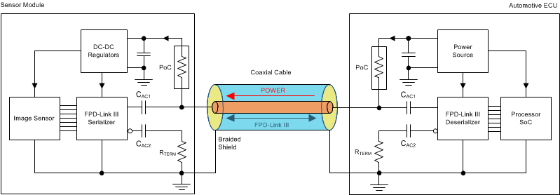
The DS90UB638-Q1 is designed to support the Power-over-Coax (PoC) method of powering remote sensor systems. With this method, the power is delivered over the same medium (a coaxial cable) used for high-speed digital video data and bidirectional control and diagnostics data transmission. The method uses passive networks or filters that isolate the transmission line from the loading of the DC/DC regulator circuits and their connecting power traces on both sides of the link as shown in #SNLS47910566.
 Figure 8-1 Power-over-Coax (PoC) System
Diagram
Figure 8-1 Power-over-Coax (PoC) System
DiagramThe PoC networks' impedance of ≥ 1 kΩ over a specific frequency band is recommended to isolate the transmission line from the loading of the regulator circuits. Higher PoC network impedance will contribute to favorable insertion loss and return loss characteristics in the high-speed channel. The lower limit of the frequency band is defined as ½ of the frequency of the back channel, fBC. The upper limit of the frequency band is the frequency of the forward high-speed channel, fFC. However, the main criteria that need to be met in the total high-speed channel, which consists of a serializer PCB, a deserializer PCB, and a cable, are the insertion loss and return loss limits defined in the Total Channel Requirements, while the system is under maximum current load and extreme temperature conditions#X123333#GUID-8667EFDD-57CE-44FD-BBD6-65D2BF97AE31.
|
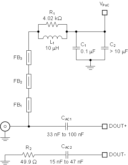
#SNLS47910566A shows a PoC network recommended for a 4G FPD-Link III consisting of DS90UB63x-Q1 CSI-2 and DS90UB638-Q1 pair with the bidirectional channel operating at 50 Mbps (fBCC = 50 MHz) and the forward channel operating at 4.16 Gbps (fFC ≈ 2 GHz).
 Figure 8-2 Typical PoC Network for a 4 Gbps FPD-Link III
Table 8-1 lists essential components for this particular PoC network.
| COUNT | REF DES | DESCRIPTION | PART NUMBER | MFR |
|---|---|---|---|---|
| 1 | L1 | Inductor, 10 µH, 0.288 Ω maximum, 530 mA minimum
(Isat, Itemp) 30-MHz SRF min, 3 mm × 3 mm, General-Purpose |
LQH3NPN100MJR | Murata |
| Inductor, 10 µH, 0.288 Ω maximum, 530 mA minimum
(Isat, Itemp) 30-MHz SRF min, 3 mm × 3 mm, AEC-Q200 |
LQH3NPZ100MJR | Murata | ||
| Inductor, 10 µH, 0.360 Ω maximum, 450 mA minimum
(Isat, Itemp) 30-MHz SRF min, 3.2 mm × 2.5 mm, AEC-Q200 |
NLCV32T-100K-EFD | TDK | ||
| Inductor, 10 µH, 0.400 Ω typical, 550 mA minimum
(Isat, Itemp) 39-MHz SRF typ, 3 mm × 3 mm, AEC-Q200 |
TYS3010100M-10 | Laird | ||
| Inductor, 10 µH, 0.325 Ω maximum, 725 mA minimum
(Isat, Itemp) 41-MHz SRF typ, 3 mm × 3 mm, AEC-Q200 |
TYS3015100M-10 | Laird | ||
| 3 | FB1-FB3 | Ferrite Bead, 1.5 kΩ at 1 GHz, 0.5 Ω maximum at
DC 500 mA at 85°C, SM0603, General Purpose |
BLM18HE152SN1 | Murata |
| Ferrite Bead, 1.5 kΩ at 1 GHz, 0.5 Ω maximum at
DC 500 mA at 85°C, SM0603, AEC-Q200 |
BLM18HE152SZ1 | Murata |
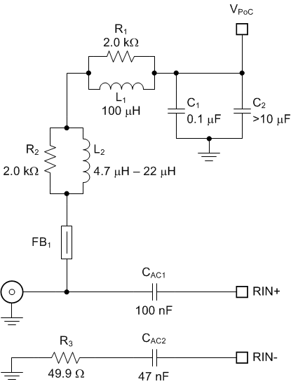
#SNLS47910566B shows a PoC network recommended for a 2G FPD-Link III consisting of a DS90UB633A-Q1 serializer and DS90UB638-Q1 with the bidirectional channel operating at the data rate of 2.5 Mbps (½ fBCC = 2.5 MHz) and the forward channel operating at the data rate as high as 1.87 Gbps (fFC ≈ 1 GHz).
 Figure 8-3 Typical PoC Network for a 2G
FPD-Link III
Figure 8-3 Typical PoC Network for a 2G
FPD-Link IIITable 8-2 lists essential components for this particular PoC network.
| COUNT | REF DES | DESCRIPTION | PART NUMBER | MFR |
|---|---|---|---|---|
| 1 | L1 | Inductor, 100 µH, 0.310 Ω maximum, 710 mA minimum
(Isat, Itemp) 7.2-MHz SRF typical, 6.6 mm × 6.6 mm, AEC-Q200 |
MSS7341-104ML | Coilcraft |
| 1 | L2 | Inductor, 4.7 µH, 0.350 Ω maximum, 700 mA minimum
(Isat, Itemp) 160-MHz SRF typical, 3.8 mm x 3.8 mm, AEC-Q200 |
1008PS-472KL | Coilcraft |
| Inductor, 4.7 µH, 0.130 Ω maximum, 830 mA minimum
(Isat, Itemp), 70-MHz SRF typical, 3.2 mm × 2.5 mm, AEC-Q200 |
CBC3225T4R7MRV | Taiyo Yuden | ||
| 1 | FB1 | Ferrite Bead, 1.5 kΩ at 1 GHz, 0.5 Ω maximum at
DC 500-mA at 85°C, SM0603, General-Purpose |
BLM18HE152SN1 | Murata |
| Ferrite Bead, 1.5 kΩ at 1 GHz, 0.5 Ω maximum at
DC 500-mA at 85°C, SM0603, AEC-Q200 |
BLM18HE152SZ1 | Murata |
Application report Power-over-Coax Design Guidelines for DS90UB953-Q1 (SNLA272) discusses PoC networks in more detail.
In addition to the PoC network components selection, their placement and layout play a critical role as well.
- Place the smallest component, typically a ferrite bead or a chip inductor, as close to the connector as possible. Route the high-speed trace through one of its pads to avoid stubs.
- Use the smallest component pads as allowed by manufacturer's design rules. Add anti-pads in the inner planes below the component pads to minimize impedance drop.
- Consult with the connector manufacturer for the optimized connector footprint. If the connector is mounted on the same side as the IC, minimize the impact of the through-hole connector stubs by routing the high-speed signal traces on the opposite side of the connector mounting side.
- Use coupled 100-Ω differential signal traces from the device pins to the AC-coupling caps. Use 50-Ω single-ended traces from the AC-coupling capacitors to the connector.
- Terminate the inverting signal traces close to the connectors with standard 49.9-Ω resistors.
The suggested characteristics for single-ended PCB traces (microstrips or striplines) for serializer or deserializer boards are detailed in Table 8-3. The effects of the PoC networks must be accounted for when testing the traces for compliance to the suggested limits.
| PARAMETER | MIN | TYP | MAX | UNIT | ||
|---|---|---|---|---|---|---|
| Ltrace | Single-ended PCB trace length from the device pin to the connector pin | 5 | cm | |||
| Ztrace | Single-ended PCB trace characteristic impedance | 45 | 50 | 55 | Ω | |
| Zcon | Connector (mounted) characteristic impedance | 40 | 50 | 60 | Ω | |
| tΔZ_con | Allowable electrical length of the connector impedance discontinuity as measured with a TDR (100 ps edge) | 20 | ps | |||
The VPOC noise must be kept 10 mVp-p or lower on the source / deserializer side of the system. The VPOC fluctuations on the serializer side, caused by the transient current draw of the sensor and the DC resistance of cables and PoC components, must be kept at minimum as well. Increasing the VPOC voltage and adding extra decoupling capacitance (> 10 µF) help reduce the amplitude and slew rate of the VPOC fluctuations.