ZHCSIS3B September   2018  – December 2022 DP83869HM

PRODUCTION DATA  

  1. 特性
  2. 应用
  3. 说明
  4. Revision History
  5. 说明(续)
  6. Device Comparison Table
  7. Pin Configuration and Functions
  8. Specifications
    1. 8.1 Absolute Maximum Ratings
    2. 8.2 ESD Ratings
    3. 8.3 Recommended Operating Conditions
    4. 8.4 Thermal Information
    5. 8.5 Electrical Characteristics
    6. 8.6 Timing Requirements
    7. 8.7 Timing Diagrams
    8. 8.8 Typical Characteristics
  9. Detailed Description
    1. 9.1 Overview
    2. 9.2 Functional Block Diagram
    3. 9.3 Feature Description
      1. 9.3.1  WoL (Wake-on-LAN) Packet Detection
        1. 9.3.1.1 Magic Packet Structure
        2. 9.3.1.2 Magic Packet Example
        3. 9.3.1.3 Wake-on-LAN Configuration and Status
      2. 9.3.2  Start of Frame Detect for IEEE 1588 Time Stamp
        1. 9.3.2.1 SFD Latency Variation and Determinism
          1. 9.3.2.1.1 1000-Mb SFD Variation in Master Mode
          2. 9.3.2.1.2 1000-Mb SFD Variation in Slave Mode
          3. 9.3.2.1.3 100-Mb SFD Variation
      3. 9.3.3  Clock Output
      4. 9.3.4  Loopback Mode
        1. 9.3.4.1 Near-End Loopback
          1. 9.3.4.1.1 MII Loopback
          2. 9.3.4.1.2 PCS Loopback
          3. 9.3.4.1.3 Digital Loopback
          4. 9.3.4.1.4 Analog Loopback
          5. 9.3.4.1.5 External Loopback
          6. 9.3.4.1.6 Far-End (Reverse) Loopback
        2.       39
      5. 9.3.5  BIST Configuration
      6. 9.3.6  Interrupt
      7. 9.3.7  Power-Saving Modes
        1. 9.3.7.1 IEEE Power Down
        2. 9.3.7.2 Active Sleep
        3. 9.3.7.3 Passive Sleep
      8. 9.3.8  Mirror Mode
      9. 9.3.9  Speed Optimization
      10. 9.3.10 Cable Diagnostics
        1. 9.3.10.1 TDR
      11. 9.3.11 Fast Link Drop
      12. 9.3.12 Jumbo Frames
    4. 9.4 Device Functional Modes
      1. 9.4.1  Copper Ethernet
        1. 9.4.1.1 1000BASE-T
        2. 9.4.1.2 100BASE-TX
        3. 9.4.1.3 10BASE-Te
      2. 9.4.2  Fiber Ethernet
        1. 9.4.2.1 1000BASE-X
        2. 9.4.2.2 100BASE-FX
      3. 9.4.3  Serial GMII (SGMII)
      4. 9.4.4  Reduced GMII (RGMII)
        1. 9.4.4.1 1000-Mbps Mode Operation
        2. 9.4.4.2 1000-Mbps Mode Timing
        3. 9.4.4.3 10- and 100-Mbps Mode
      5. 9.4.5  Media Independent Interface (MII)
      6. 9.4.6  Bridge Modes
        1. 9.4.6.1 RGMII-to-SGMII Mode
        2. 9.4.6.2 SGMII-to-RGMII Mode
        3.       69
      7. 9.4.7  Media Convertor Mode
      8. 9.4.8  Register Configuration for Operational Modes
        1. 9.4.8.1 RGMII-to-Copper Ethernet Mode
        2. 9.4.8.2 RGMII-to-1000Base-X Mode
        3. 9.4.8.3 RGMII-to-100Base-FX Mode
        4. 9.4.8.4 RGMII-to-SGMII Bridge Mode
        5. 9.4.8.5 1000M Media Convertor Mode
        6. 9.4.8.6 100M Media Convertor Mode
        7. 9.4.8.7 SGMII-to-Copper Ethernet Mode
      9. 9.4.9  Serial Management Interface
        1. 9.4.9.1 Extended Address Space Access
          1. 9.4.9.1.1 Write Address Operation
          2. 9.4.9.1.2 Read Address Operation
          3. 9.4.9.1.3 Write (No Post Increment) Operation
          4. 9.4.9.1.4 Read (No Post Increment) Operation
          5. 9.4.9.1.5 Write (Post Increment) Operation
          6. 9.4.9.1.6 Read (Post Increment) Operation
          7. 9.4.9.1.7 Example of Read Operation Using Indirect Register Access
          8. 9.4.9.1.8 Example of Write Operation Using Indirect Register Access
      10. 9.4.10 Auto-Negotiation
        1. 9.4.10.1 Speed and Duplex Selection - Priority Resolution
        2. 9.4.10.2 Master and Slave Resolution
        3. 9.4.10.3 Pause and Asymmetrical Pause Resolution
        4. 9.4.10.4 Next Page Support
        5. 9.4.10.5 Parallel Detection
        6. 9.4.10.6 Restart Auto-Negotiation
        7. 9.4.10.7 Enabling Auto-Negotiation Through Software
        8. 9.4.10.8 Auto-Negotiation Complete Time
        9. 9.4.10.9 Auto-MDIX Resolution
    5. 9.5 Programming
      1. 9.5.1 Strap Configuration
        1. 9.5.1.1 Straps for PHY Address
        2. 9.5.1.2 Strap for DP83869HM Functional Mode Selection
        3. 9.5.1.3 LED Default Configuration Based on Device Mode
        4. 9.5.1.4 Straps for RGMII/SGMII to Copper
        5. 9.5.1.5 Straps for RGMII to 1000Base-X
        6. 9.5.1.6 Straps for RGMII to 100Base-FX
        7. 9.5.1.7 Straps for Bridge Mode (SGMII-RGMII)
        8. 9.5.1.8 Straps for 100M Media Convertor
        9. 9.5.1.9 Straps for 1000M Media Convertor
      2. 9.5.2 LED Configuration
      3. 9.5.3 Reset Operation
        1. 9.5.3.1 Hardware Reset
        2. 9.5.3.2 IEEE Software Reset
        3. 9.5.3.3 Global Software Reset
        4. 9.5.3.4 Global Software Restart
    6. 9.6 Register Maps
      1. 9.6.1 DP83869 Registers
  10. 10Application and Implementation
    1. 10.1 Application Information
    2. 10.2 Typical Applications
      1. 10.2.1 Copper Ethernet Typical Application
        1. 10.2.1.1 Design Requirements
        2. 10.2.1.2 Detailed Design Procedure
          1. 10.2.1.2.1 Clock Input
            1. 10.2.1.2.1.1 Crystal Recommendations
            2. 10.2.1.2.1.2 External Clock Source Recommendation
          2. 10.2.1.2.2 Magnetics Requirements
            1. 10.2.1.2.2.1 Magnetics Connection
        3. 10.2.1.3 Application Curves
      2. 10.2.2 Fiber Ethernet Typical Ethernet
        1. 10.2.2.1 Design Requirements
        2. 10.2.2.2 Detailed Design Procedure
          1. 10.2.2.2.1 Transceiver Connections
        3. 10.2.2.3 Application Curves
  11. 11Power Supply Recommendations
    1. 11.1 Two-Supply Configuration
    2. 11.2 Three-Supply Configuration
  12. 12Layout
    1. 12.1 Layout Guidelines
      1. 12.1.1 Signal Traces
        1. 12.1.1.1 MAC Interface Layout Guidelines
          1. 12.1.1.1.1 SGMII Layout Guidelines
          2. 12.1.1.1.2 RGMII Layout Guidelines
        2. 12.1.1.2 MDI Layout Guidelines
      2. 12.1.2 Return Path
      3. 12.1.3 Transformer Layout
      4. 12.1.4 Metal Pour
      5. 12.1.5 PCB Layer Stacking
    2. 12.2 Layout Example
  13. 13Device and Documentation Support
    1. 13.1 Documentation Support
      1. 13.1.1 Related Documentation
    2. 13.2 Receiving Notification of Documentation Updates
    3. 13.3 支持资源
    4. 13.4 Trademarks
    5. 13.5 Electrostatic Discharge Caution
    6. 13.6 术语表
  14. 14Mechanical, Packaging, and Orderable Information

封装选项

机械数据 (封装 | 引脚)
散热焊盘机械数据 (封装 | 引脚)
订购信息
Crystal Recommendations

A 25-MHz, parallel, 15-pF to 40-pF load crystal resonator should be used if a crystal source is desired. Figure 10-2 shows a typical connection for a crystal resonator circuit. The load capacitor values vary with the crystal vendors. Check with the vendor for the recommended loads.
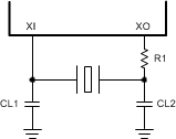
GUID-E4D032EA-5D4E-4791-99A2-84D5FDB84697-low.gifFigure 10-2 Crystal Oscillator Circuit

As a starting point for evaluating the oscillator performance, the value of CL1 and CL2 should each be equal to 2x the specified load capacitance from the crystal vendor’s data sheet. For example, if the specified load capacitance of the crystal is 10 pF, set CL1 = CL2 = 20 pF. CL1, CL2 value may need to be adjusted based on the parasitic capacitance. Depending on the crystal drive level, R1 may or may not be needed.

Specification for 25-MHz crystal are listed in Table 10-1.

Table 10-1 25-MHz Crystal Specifications
PARAMETERTEST CONDITIONMINTYPMAXUNIT
Frequency25MHz
Frequency ToleranceIncluding Operational Temperature, Aging, and Other Factors±100ppm
Load Capacitance1540pF
ESR50ohm