ZHCSNO0B April   2021  – November 2021 DP83561-SP

PRODUCTION DATA  

  1. 特性
  2. 应用
  3. 说明
  4. Revision History
  5. Pin Configuration and Functions
    1. 5.1 Pin States
  6. Specifications
    1. 6.1 Absolute Maximum Ratings
    2. 6.2 ESD Ratings
    3. 6.3 Recommended Operating Conditions
    4. 6.4 Thermal Information
    5. 6.5 Electrical Characteristics
    6. 6.6 Timing Requirements
      1. 6.6.1 Timing Requirement Diagrams
    7. 6.7 Typical Characteristics
  7. Detailed Description
    1. 7.1 Overview
      1. 7.1.1 Engineering Model (Parts With /EM Suffix)
    2. 7.2 Functional Block Diagram
    3. 7.3 Feature Description
      1. 7.3.1 Copper Ethernet
        1. 7.3.1.1 1000BASE-T
        2. 7.3.1.2 100BASE-TX
        3. 7.3.1.3 10BASE-Te
      2. 7.3.2 MAC Interfaces
        1. 7.3.2.1 Reduced GMII (RGMII)
          1. 7.3.2.1.1 RGMII-TX Requirements
          2. 7.3.2.1.2 RGMII-RX Requirements
          3. 7.3.2.1.3 1000-Mbps Mode Operation
          4. 7.3.2.1.4 1000-Mbps Mode Timing
          5. 7.3.2.1.5 10- and 100-Mbps Mode
        2. 7.3.2.2 Media Independent Interface (MII)
      3. 7.3.3 Auto-Negotiation
        1. 7.3.3.1 Speed and Duplex Selection - Priority Resolution
        2. 7.3.3.2 Master and Slave Resolution
        3. 7.3.3.3 Pause and Asymmetrical Pause Resolution
        4. 7.3.3.4 Next Page Support
        5. 7.3.3.5 Parallel Detection
        6. 7.3.3.6 Restart Auto-Negotiation
        7. 7.3.3.7 Enabling Auto-Negotiation Through Software
        8. 7.3.3.8 Auto-Negotiation Complete Time
        9. 7.3.3.9 Auto-MDIX Resolution
      4. 7.3.4 Speed Optimization
      5. 7.3.5 Radiation Performance
        1. 7.3.5.1 Total Ionizing Dose (TID)
        2. 7.3.5.2 Single-Event Effects (SEE)
        3. 7.3.5.3 Single Event Functional Interrupt (SEFI) Monitor Suite
          1. 7.3.5.3.1 PCS State Machine Monitors
          2. 7.3.5.3.2 Configuration Register Monitors
          3. 7.3.5.3.3 Temperature Monitor
          4. 7.3.5.3.4 PLL Lock Monitor
      6. 7.3.6 WoL (Wake-on-LAN) Packet Detection
        1. 7.3.6.1 Magic Packet Structure
        2. 7.3.6.2 Magic Packet Example
        3. 7.3.6.3 Wake-on-LAN Configuration and Status
      7. 7.3.7 Start of Frame Detect for IEEE 1588 Time Stamp
        1. 7.3.7.1 SFD Latency Variation and Determinism
          1. 7.3.7.1.1 1000M SFD Variation in Master Mode
          2. 7.3.7.1.2 1000M SFD Variation in Slave Mode
          3. 7.3.7.1.3 100M SFD Variation
      8. 7.3.8 Cable Diagnostics
        1. 7.3.8.1 TDR
        2. 7.3.8.2 Fast Link Drop
        3. 7.3.8.3 Fast Link Detect
        4. 7.3.8.4 Energy Detect
        5. 7.3.8.5 IEEE 802.3 Test Modes
        6. 7.3.8.6 Jumbo Frames
      9. 7.3.9 Clock Output
    4. 7.4 Device Functional Modes
      1. 7.4.1 Mirror Mode
      2. 7.4.2 Loopback Mode
        1. 7.4.2.1 Near-End Loopback
          1. 7.4.2.1.1 MII Loopback
          2. 7.4.2.1.2 PCS Loopback
          3. 7.4.2.1.3 Digital Loopback
          4. 7.4.2.1.4 Analog Loopback
          5. 7.4.2.1.5 External Loopback
          6. 7.4.2.1.6 Far-End (Reverse) Loopback
        2. 7.4.2.2 Loopback Availability Exception
      3. 7.4.3 Power-Saving Modes
        1. 7.4.3.1 IEEE Power Down
        2. 7.4.3.2 Deep Power-Down Mode
        3. 7.4.3.3 Active Sleep
        4. 7.4.3.4 Passive Sleep
    5. 7.5 Programming
      1. 7.5.1 Serial Management Interface
        1. 7.5.1.1 Extended Address Space Access
          1. 7.5.1.1.1 Write Address Operation
          2. 7.5.1.1.2 Read Address Operation
          3. 7.5.1.1.3 Write (No Post Increment) Operation
          4. 7.5.1.1.4 Read (No Post Increment) Operation
          5. 7.5.1.1.5 Write (Post Increment) Operation
          6. 7.5.1.1.6 Read (Post Increment) Operation
          7. 7.5.1.1.7 Example of Read Operation Using Indirect Register Access
          8. 7.5.1.1.8 Example of Write Operation Using Indirect Register Access
      2. 7.5.2 Interrupt
      3. 7.5.3 BIST Configuration
      4. 7.5.4 Strap Configuration
      5. 7.5.5 LED Configuration
      6. 7.5.6 LED Operation From 1.8-V I/O VDD Supply
      7. 7.5.7 Reset Operation
        1. 7.5.7.1 Hardware Reset
        2. 7.5.7.2 IEEE Software Reset
        3. 7.5.7.3 Global Software Reset
        4. 7.5.7.4 Global Software Restart
        5. 7.5.7.5 PCS Restart
    6. 7.6 Register Maps
      1. 7.6.1 DP83561SP Registers
  8. Application and Implementation
    1. 8.1 Application Information
    2. 8.2 Typical Application
      1. 8.2.1 Design Requirements
      2. 8.2.2 Detailed Design Procedure
        1. 8.2.2.1 Clock Input
          1. 8.2.2.1.1 Crystal Recommendations
          2. 8.2.2.1.2 External Clock Source Recommendations
        2. 8.2.2.2 MAC Interface
          1. 8.2.2.2.1 RGMII Layout Guidelines
          2. 8.2.2.2.2 MII Layout Guidelines
        3. 8.2.2.3 Media Dependent Interface (MDI)
          1. 8.2.2.3.1 MDI Layout Guidelines
        4. 8.2.2.4 Magnetics Requirements
          1. 8.2.2.4.1 Magnetics Connection
  9. Power Supply Recommendations
    1. 9.1 Two-Supply Configuration
    2. 9.2 Three-Supply Configuration
  10. 10Layout
    1. 10.1 Layout Guidelines
      1. 10.1.1 Signal Traces
      2. 10.1.2 Return Path
      3. 10.1.3 Transformer Layout
      4. 10.1.4 Metal Pour
      5. 10.1.5 PCB Layer Stacking
    2. 10.2 Layout Example
  11. 11Device and Documentation Support
    1. 11.1 Documentation Support
      1. 11.1.1 Related Documentation
    2. 11.2 接收文档更新通知
    3. 11.3 支持资源
    4. 11.4 Trademarks
    5. 11.5 Electrostatic Discharge Caution
    6. 11.6 术语表
  12. 12Mechanical, Packaging, and Orderable Information

封装选项

机械数据 (封装 | 引脚)
散热焊盘机械数据 (封装 | 引脚)
订购信息

Magic Packet Structure

When configured for Magic Packet mode, the DP83561-SP scans all incoming frames addressed to the node for a specific data sequence. This sequence identifies the frame as a Magic Packet frame.

Note:

The Magic Packet should be byte aligned.

A Magic Packet frame must also meet the basic requirements for the LAN technology chosen, such as SOURCE ADDRESS, DESTINATION ADDRESS (which may be the receiving station’s IEEE address or a BROADCAST address), and CRC.

The specific Magic Packet sequence consists of 16 duplications of the IEEE address of this node, with no breaks or interruptions, followed by secure-on password if security is enabled. This sequence can be located anywhere within the packet, but must be preceded by a synchronization stream. The synchronization stream is defined as 6 bytes of FFh.
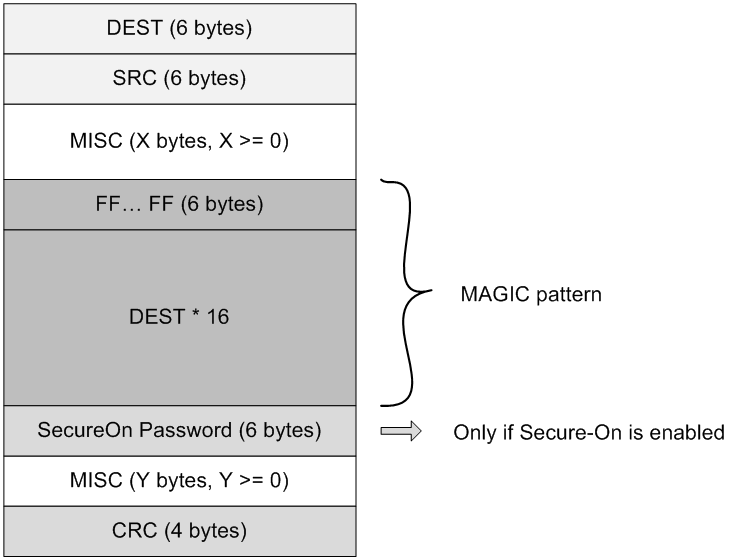
GUID-64942F81-8CB5-4435-937D-14C79BA0B7F8-low.gifFigure 7-6 Magic Packet Structure