ZHCSI46C April 2018 – December 2020 DLPC3470
PRODUCTION DATA
- 1 特性
- 2 应用
- 3 说明
- 4 Revision History
- 5 Pin Configuration and Functions
-
6 Specifications
- 6.1 Absolute Maximum Ratings
- 6.2 ESD Ratings
- 6.3 Recommended Operating Conditions
- 6.4 Thermal Information
- 6.5 Power Electrical Characteristics
- 6.6 Pin Electrical Characteristics
- 6.7 Internal Pullup and Pulldown Electrical Characteristics
- 6.8 DMD Sub-LVDS Interface Electrical Characteristics
- 6.9 DMD Low-Speed Interface Electrical Characteristics
- 6.10 System Oscillator Timing Requirements
- 6.11 Power Supply and Reset Timing Requirements
- 6.12 Parallel Interface Frame Timing Requirements
- 6.13 Parallel Interface General Timing Requirements
- 6.14 BT656 Interface General Timing Requirements
- 6.15 Flash Interface Timing Requirements
- 6.16 Other Timing Requirements
- 6.17 DMD Sub-LVDS Interface Switching Characteristics
- 6.18 DMD Parking Switching Characteristics
- 6.19 Chipset Component Usage Specification
-
7 Detailed Description
- 7.1 Overview
- 7.2 Functional Block Diagram
- 7.3 Feature Description
- 7.4 Device Functional Modes
- 7.5 Programming
- 8 Application and Implementation
- 9 Power Supply Recommendations
- 10Layout
- 11Device and Documentation Support
- 12Mechanical, Packaging, and Orderable Information
7.3.10.1 Sub-LVDS (HS) Interface
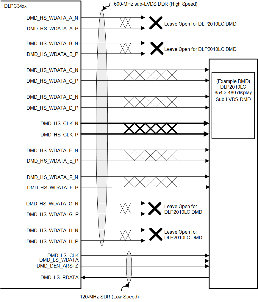
The DLP2010LC and DLP2010NIR (.2 WVGA) DMDs do not require all of the available output data lanes of the controller. Internal software selection allows the controller to support multiple DMD interface swap configurations. These options can improve board layout by remapping specific combinations of DMD interface lines to other DMD interface lines as needed. Table 7-10 shows the four options available for the DLP2010LC DMD. Leave any unused DMD signal pairs unconnected on the final board design.
| DLP2010LC 4-LANE DMD ROUTING OPTIONS | DMD PINS | |||
|---|---|---|---|---|
| OPTION 1 | OPTION 2 | OPTION 3 | OPTION 4 | |
| HS_WDATA_D_P HS_WDATA_D_N | HS_WDATA_E_P HS_WDATA_E_N | HS_WDATA_H_P HS_WDATA_H_N | HS_WDATA_A_P HS_WDATA_A_N | Input DATA_P_0 Input DATA_N_0 |
| HS_WDATA_C_P HS_WDATA_C_N | HS_WDATA_F_P HS_WDATA_F_N | HS_WDATA_G_P HS_WDATA_G_N | HS_WDATA_B_P HS_WDATA_B_N | Input DATA_P_1 Input DATA_N_1 |
| HS_WDATA_F_P HS_WDATA_F_N | HS_WDATA_C_P HS_WDATA_C_N | HS_WDATA_B_P HS_WDATA_B_N | HS_WDATA_G_P HS_WDATA_G_N | Input DATA_P_2 Input DATA_N_2 |
| HS_WDATA_E_P HS_WDATA_E_N | HS_WDATA_D_P HS_WDATA_D_N | HS_WDATA_A_P HS_WDATA_A_N | HS_WDATA_H_P HS_WDATA_H_N | Input DATA_P_3 Input DATA_N_3 |
 Figure 7-23 DLP2010LC (.2 WVGA) DMD
Interface Example (Option 1 and 2)
Figure 7-23 DLP2010LC (.2 WVGA) DMD
Interface Example (Option 1 and 2)The sub-LVDS high-speed interface waveform quality and timing on the DLPC34xx controller depends on the total length of the interconnect system, the spacing between traces, the characteristic impedance, etch losses, and how well matched the lengths are across the interface. Thus, ensuring positive timing margin requires attention to many factors.
In an attempt to minimize the signal integrity analysis that would otherwise be required, the DMD Control and Sub-LVDS Signals layout section is provided as a reference of an interconnect system that satisfy both waveform quality and timing requirements (accounting for both PCB routing mismatch and PCB signal integrity). Variation from these recommendations may also work, but should be confirmed with PCB signal integrity analysis or lab measurements.