ZHCSI46C April 2018 – December 2020 DLPC3470
PRODUCTION DATA
- 1 特性
- 2 应用
- 3 说明
- 4 Revision History
- 5 Pin Configuration and Functions
-
6 Specifications
- 6.1 Absolute Maximum Ratings
- 6.2 ESD Ratings
- 6.3 Recommended Operating Conditions
- 6.4 Thermal Information
- 6.5 Power Electrical Characteristics
- 6.6 Pin Electrical Characteristics
- 6.7 Internal Pullup and Pulldown Electrical Characteristics
- 6.8 DMD Sub-LVDS Interface Electrical Characteristics
- 6.9 DMD Low-Speed Interface Electrical Characteristics
- 6.10 System Oscillator Timing Requirements
- 6.11 Power Supply and Reset Timing Requirements
- 6.12 Parallel Interface Frame Timing Requirements
- 6.13 Parallel Interface General Timing Requirements
- 6.14 BT656 Interface General Timing Requirements
- 6.15 Flash Interface Timing Requirements
- 6.16 Other Timing Requirements
- 6.17 DMD Sub-LVDS Interface Switching Characteristics
- 6.18 DMD Parking Switching Characteristics
- 6.19 Chipset Component Usage Specification
-
7 Detailed Description
- 7.1 Overview
- 7.2 Functional Block Diagram
- 7.3 Feature Description
- 7.4 Device Functional Modes
- 7.5 Programming
- 8 Application and Implementation
- 9 Power Supply Recommendations
- 10Layout
- 11Device and Documentation Support
- 12Mechanical, Packaging, and Orderable Information
7.3.2.2.2 Trigger In Mode
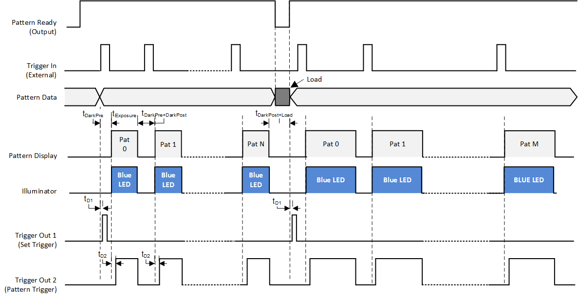
Trigger In mode provides higher level of control to the user for displaying patterns. In this mode, the user determines when to display the pattern by sending an external trigger signal to the DLPC3470 controller. The DLPC3470 controller outputs a Pattern Ready signal to let the user know when DLPC3470 controller is ready to accept an external trigger signal.
 Figure 7-15 Trigger In Mode
- The DLPC3470 controller sets the Pattern Ready signal high to denote that the DLPC3470 controller is ready to accept the Trigger In signal.
- The user sends the external trigger input signal to the DLPC3470 controller to begin the display of the next pattern with tExposure (exposure time), tDarkPre and tDarkPost (dark time).
- The Blue LED is configured to be on for each pattern.
- TRIG_OUT_1 (Pattern Set Trigger) is configured active high polarity and will have a minimum pulse width of 20 microseconds. TRIG_OUT_1 delay (tD1) is configured with respect to external trigger input (TRIG_IN).
- TRIG_OUT_2 (Pattern Trigger) is configured active high polarity and stays active during the pattern exposure. TRIG_OUT_2 delay (tD2) is configured with reference to the start of each pattern exposure.