ZHCSR35A November 2019 – August 2020 BQ79600-Q1
PRODUCTION DATA
- 1 特性
- 2 应用
- 3 说明
- 4 Revision History
- 5 Pin Configuration and Functions
- 6 规格
-
7 Detailed Description
- 7.1 Overview
- 7.2 Functional Block Diagram
- 7.3
Feature Description
- 7.3.1 Functional Modes and Power Supply
- 7.3.2 Communication
- 7.3.3 Fault Handling
- 7.3.4 INH/ Reverse Wakeup
- 7.3.5 Sniff Detector
- 7.3.6 Device Diagnostic
- 7.4 Device Functional Modes
- 7.5
Register Maps
- 7.5.1 Register Summary Table
- 7.5.2 Register: DIR0_ADDR
- 7.5.3 Register: DIR1_ADDR
- 7.5.4 Register: CONTROL1
- 7.5.5 Register: CONTROL2
- 7.5.6 Register: DIAG_CTRL
- 7.5.7 Register: DEV_CONF1
- 7.5.8 Register: DEV_CONF2
- 7.5.9 Register: TX_HOLD_OFF
- 7.5.10 Register: SLP_TIMEOUT
- 7.5.11 Register: COMM_TIMEOUT
- 7.5.12 Register: SPI_FIFO_UNLOCK
- 7.5.13 Register: FAULT_MSK
- 7.5.14 Register: FAULT_RST
- 7.5.15 Register: FAULT_SUMMARY
- 7.5.16 Register: FAULT_REG
- 7.5.17 Register: FAULT_SYS
- 7.5.18 Register: FAULT_PWR
- 7.5.19 Register: FAULT_COMM1
- 7.5.20 Register: FAULT_COMM2
- 7.5.21 Register: DEV_DIAG_STAT
- 7.5.22 Register: PARTID
- 7.5.23 Register: DIE_ID1
- 7.5.24 Register: DIE_ID2
- 7.5.25 Register: DIE_ID3
- 7.5.26 Register: DIE_ID4
- 7.5.27 Register: DIE_ID5
- 7.5.28 Register: DIE_ID6
- 7.5.29 Register: DIE_ID7
- 7.5.30 Register: DIE_ID8
- 7.5.31 Register: DIE_ID9
- 7.5.32 Register: DEBUG_CTRL_UNLOCK
- 7.5.33 Register: DEBUG_COMM_CTRL
- 7.5.34 Register: DEBUG_COMM_STAT
- 7.5.35 Register: DEBUG_SPI_PHY
- 7.5.36 Register: DEBUG_SPI_FRAME
- 7.5.37 Register: DEBUG_UART_FRAME
- 7.5.38 Register: DEBUG_COMH_PHY
- 7.5.39 Register: DEBUG_COMH_FRAME
- 7.5.40 Register: DEBUG_COML_PHY
- 7.5.41 Register: DEBUG_COML_FRAME
- 8 Application and Implementation
- 9 Power Supply Recommendations
- 10Layout
- 11Device and Documentation Support
- 12Mechanical, Packaging, and Orderable Information
7.3.2.1.1 Frame Layer
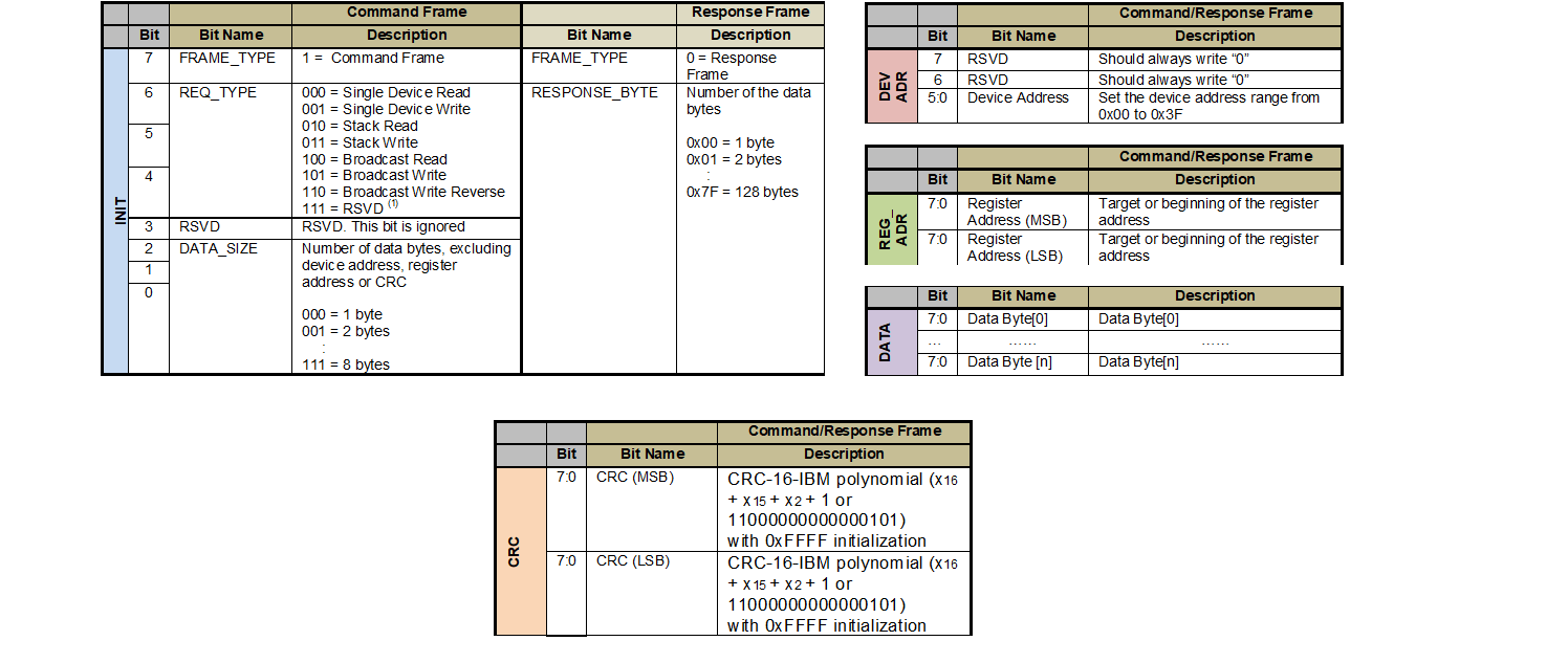
The communication frame is defined in figure below. It is made up of 5 types of information: initialization character (INIT), device address characters, register address character, data character(s) and CRC characters. Each character is transmitted at UART/ SPI/ Daisy Chain physical level, whose format is defined in following Section 7.3.2.1.2 section. There are 3 types of transaction frames: Read Command Frames, Write Command Frames and Response Frames. They follow the structure in the figure below.
 Figure 7-7 Command/Response Frame Structure
Notes:
- When BQ79600-Q1 is used as bridge device, to read BQ devices information, host SHALL NOT use Broadcast Read command but only Single Device Read or Stack Read. The reason is BQ79600-Q1 register address does not overlap with stack devices, it would only return 0x00 to Broadcast Read command.
- For Stack Read command, the response is broken into individual response frames from each device addressed. Each device (address N) in the stack waits until the device above it (address N+1) responds before device N sends its own data back.
- After a read command frame is transmitted, the host must wait for all expected responses to return (or timeout: tWAIT_READ_MAX ) before initiating a new command frame.
- A response frame is not mandatary. A response frame is only received after a read command frame.
- Broadcast Write Reverse command frame should only be used to config [DIR_SEL] bit, not for any other purposes. INIT byte is 0xE0, Reg address byte is 0x309 (BQ7961X-Q1), data byte is 0x80.
- Bytes received on COMH/COML are NOT propagated up to the stack; while bytes received on the SPI/UART are propagated to COMH or COML depending on [DIR_SEL].
- Even if there is a byte error, data is still forwarded from VIF to SPI (buffer)/UART; if there is a byte error, data doesn’t forward from SPI/UART to VIF.
 Figure 7-8 Frame Byte Definition
Notes:
- INIT character: (1) No function to this selection, but this selection sets the [RC_IERR] error flag.
- Device Address character: Bit 6 and 7 are reserved; 0x4F to 0xFF is decoded as 0x3F by device.
- Register Address characters: Register addresses are two bytes in length. They indicate the targeted register address on a single byte read/write, or the beginning of the register address on a multi-byte read/write. If an invalid register address is set on a write command, the command will be ignored. If an invalid register address is set on a read command, a 0x00 will be returned as response.
- Data characters can be:
- Single data byte, it represents number of registers requested in Read Command Frame. The BQ79600-Q1 supports up to 128 byte reads. The valid data byte for read command frame is 0b0000000 - 0b1111111. The MSB of the data byte is ignored for read command frames. For example, 0b10011001 is read as 0b00011001 and returns data from 26 registers.
- Actual payload in Write Command Frame (max 8 byte) or Response Frame (max 128 byte).
- CRC characters:
- The CRC value is checked as the first step (assume no physical layer error, no [RC_IERR], no [RC_SOF], no [RC_BYTE_ERR]) after receiving the communication frame. If the CRC is incorrect, the entire frame is discarded and not processed. Any additional frame errors are not checked.
- The frame with CRC error is still transferred up/down the stack. Every device processing this frame will also detect a CRC error. Hence, it is possible to have multiple devices indicating CRC fault on the same communication frame. If a CRC error occurs in the response frame from address N+1, device N does NOT append its own message and an invalid CRC fault is generated. For example, if device 15 finds response frame from device 16 has invalid CRC, device 15 doesn’t send its own response frame.
-
The device uses a CRC (cyclic redundancy check) to protect data integrity during transmission. The device uses the CRC-16-IBM polynomial (x16 + x15 + x2 + 1 ) with 0xFFFF initialization.