ZHCSR35A November 2019 – August 2020 BQ79600-Q1
PRODUCTION DATA
- 1 特性
- 2 应用
- 3 说明
- 4 Revision History
- 5 Pin Configuration and Functions
- 6 规格
-
7 Detailed Description
- 7.1 Overview
- 7.2 Functional Block Diagram
- 7.3
Feature Description
- 7.3.1 Functional Modes and Power Supply
- 7.3.2 Communication
- 7.3.3 Fault Handling
- 7.3.4 INH/ Reverse Wakeup
- 7.3.5 Sniff Detector
- 7.3.6 Device Diagnostic
- 7.4 Device Functional Modes
- 7.5
Register Maps
- 7.5.1 Register Summary Table
- 7.5.2 Register: DIR0_ADDR
- 7.5.3 Register: DIR1_ADDR
- 7.5.4 Register: CONTROL1
- 7.5.5 Register: CONTROL2
- 7.5.6 Register: DIAG_CTRL
- 7.5.7 Register: DEV_CONF1
- 7.5.8 Register: DEV_CONF2
- 7.5.9 Register: TX_HOLD_OFF
- 7.5.10 Register: SLP_TIMEOUT
- 7.5.11 Register: COMM_TIMEOUT
- 7.5.12 Register: SPI_FIFO_UNLOCK
- 7.5.13 Register: FAULT_MSK
- 7.5.14 Register: FAULT_RST
- 7.5.15 Register: FAULT_SUMMARY
- 7.5.16 Register: FAULT_REG
- 7.5.17 Register: FAULT_SYS
- 7.5.18 Register: FAULT_PWR
- 7.5.19 Register: FAULT_COMM1
- 7.5.20 Register: FAULT_COMM2
- 7.5.21 Register: DEV_DIAG_STAT
- 7.5.22 Register: PARTID
- 7.5.23 Register: DIE_ID1
- 7.5.24 Register: DIE_ID2
- 7.5.25 Register: DIE_ID3
- 7.5.26 Register: DIE_ID4
- 7.5.27 Register: DIE_ID5
- 7.5.28 Register: DIE_ID6
- 7.5.29 Register: DIE_ID7
- 7.5.30 Register: DIE_ID8
- 7.5.31 Register: DIE_ID9
- 7.5.32 Register: DEBUG_CTRL_UNLOCK
- 7.5.33 Register: DEBUG_COMM_CTRL
- 7.5.34 Register: DEBUG_COMM_STAT
- 7.5.35 Register: DEBUG_SPI_PHY
- 7.5.36 Register: DEBUG_SPI_FRAME
- 7.5.37 Register: DEBUG_UART_FRAME
- 7.5.38 Register: DEBUG_COMH_PHY
- 7.5.39 Register: DEBUG_COMH_FRAME
- 7.5.40 Register: DEBUG_COML_PHY
- 7.5.41 Register: DEBUG_COML_FRAME
- 8 Application and Implementation
- 9 Power Supply Recommendations
- 10Layout
- 11Device and Documentation Support
- 12Mechanical, Packaging, and Orderable Information
7.3.2.3.2 Ring Communication (optional)
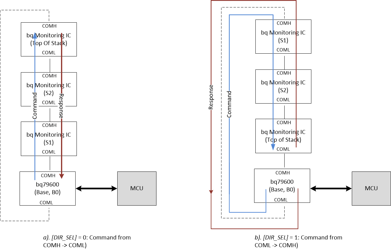
A ring communication (optional) allows the system to establish communication from either direction. This allows the system to continue communicating to all stack devices even if one piece of daisy chain cable is broken.
Table 7-10 describes a procedure auto address Figure 7-23(b): to bring up a system of 1 bridge device and 3 stack devices from SHUTDOWN to a state ready to do read/write communication in reverse direction.
To change communication direction from Figure 7-23(a) to Figure 7-23(b), follow the steps 2, 4-14. (Assuming all devices in (a) are already in ACTIVE and auto addressed as described in Table 7-9)
 Figure 7-23 Example to Change Communication Direction in Daisy Chain
| STEP | WORK WITH BQ7961X-Q1 | |
|---|---|---|
| 1 | send WAKE ping on RX (wakeup BQ79600-Q1) | |
| 2 | single device write to BQ79600-Q1 control 1 [DIR_SEL] = 1 (change BQ79600-Q1 direction) | |
| 3 | single device write to BQ79600-Q1 CONTROL1 [SEND_WAKE] = 1 (wake up stack devices) | |
| 4 | dummy stack write data 0x00 to registers 0x343 to 0x34A (sync up internal DLL). These are 8 separate write commands. | |
| 5 | brdcast write reverse 0x80 to address 0x309 (change stack devices direction DIR_SEL =1) | |
| 6 | brdcast Write 0x02 to address 0x308(1) | |
| 7 | brdcast Write 0x81 to address 0x309 (enable BQ7961X-Q1 auto addressing) | |
| 8 | brdcast Write consecutively to address 0x307 = 0,1,2,3 (address 1-3 assigned to BQ7961X-Q1, 0 assigned to BQ79600-Q1) | |
| 9 | brdcast write 0x02 to address 0x308 (set BQ7961X-Q1 as stack device ) | |
| 10 | single device write to device 3: data 0x03 to address 0x308 (set 3rd BQ7961X-Q1 as top of stack, BQ79600-Q1 is default to base) | |
| 11 | dummy stack read registers 0x343 to 0x34A (sync up internal DLL). These are 8 separate read commands. | |
| 12 | stack read address 0x307 (read back to verify address are correct for stack device) | |
| 13 | single device read to BQ79600-Q1, verify 0x2001 = 0x14 | |
| 14 | finish initialization | |