ZHCSR35A November   2019  – August 2020 BQ79600-Q1

PRODUCTION DATA  

  1. 特性
  2. 应用
  3. 说明
  4. Revision History
  5. Pin Configuration and Functions
    1.     Pin Functions
  6. 规格
    1. 6.1 Absolute Maximum Ratings
    2. 6.2 ESD Ratings
    3. 6.3 Recommended Operating Conditions
    4. 6.4 Thermal Information
    5. 6.5 Electrical Characteristics
    6. 6.6 Timing Requirements
    7. 6.7 Typical Characteristics
  7. Detailed Description
    1. 7.1 Overview
    2. 7.2 Functional Block Diagram
    3. 7.3 Feature Description
      1. 7.3.1 Functional Modes and Power Supply
        1. 7.3.1.1 Power Mode
        2. 7.3.1.2 Pings
        3. 7.3.1.3 SPI/UART 选择
        4. 7.3.1.4 Digital Reset
        5. 7.3.1.5 Power Mode in BMS System
        6. 7.3.1.6 Power Supply
        7. 7.3.1.7 Shutdown
      2. 7.3.2 Communication
        1. 7.3.2.1 Data Communication Protocol
          1. 7.3.2.1.1 Frame Layer
            1. 7.3.2.1.1.1 Calculating Frame CRC Value
            2. 7.3.2.1.1.2 Verifying Frame CRC
          2. 7.3.2.1.2 Physical Layer
            1. 7.3.2.1.2.1 UART
              1. 7.3.2.1.2.1.1 TX HOLD OFF
              2. 7.3.2.1.2.1.2 UART COMM CLEAR
            2. 7.3.2.1.2.2 SPI
              1. 7.3.2.1.2.2.1 SPI_RDY 和 SPI FIFO
              2. 7.3.2.1.2.2.2 Flow to Read/Write BQ79600-Q1
              3. 7.3.2.1.2.2.3 SPI COMM CLEAR
            3. 7.3.2.1.2.3 Daisy Chain
        2. 7.3.2.2 Tone Communication Protocol
        3. 7.3.2.3 Device Auto Addressing / Ring Communication
          1. 7.3.2.3.1 Auto-Addressing
          2. 7.3.2.3.2 Ring Communication (optional)
        4. 7.3.2.4 Communication Timeout
        5. 7.3.2.5 Communication Debug Mode
      3. 7.3.3 Fault Handling
        1. 7.3.3.1 Fault Status Hierarchy/Reset/Mask
          1. 7.3.3.1.1 Fault Status Hierarchy
          2. 7.3.3.1.2 Fault Reset and Mask
        2. 7.3.3.2 Fault Interface
          1. 7.3.3.2.1 NFAULT
          2. 7.3.3.2.2 Daisy Chain (COMH and COML)
            1. 7.3.3.2.2.1 Fault Transmitting when BQ79600-Q1 in ACTIVE
            2. 7.3.3.2.2.2 Fault Transmitting when BQ79600-Q1 in SLEEP
            3. 7.3.3.2.2.3 Fault Transmitting (Automatic Host Wakeup/Reverse Wakeup) when BQ79600-Q1 in SHUTDOWN
      4. 7.3.4 INH/ Reverse Wakeup
      5. 7.3.5 Sniff Detector
      6. 7.3.6 Device Diagnostic
        1. 7.3.6.1 Power Supplies Check
          1. 7.3.6.1.1 Power Supply Diagnostic Check
          2. 7.3.6.1.2 Power Supply BIST
        2. 7.3.6.2 Thermal Shutdown
        3. 7.3.6.3 Oscillators Watchdog
        4. 7.3.6.4 Register Bit Flip Monitor
        5. 7.3.6.5 SPI FIFO 诊断
    4. 7.4 Device Functional Modes
    5. 7.5 Register Maps
      1. 7.5.1  Register Summary Table
      2. 7.5.2  Register: DIR0_ADDR
      3. 7.5.3  Register: DIR1_ADDR
      4. 7.5.4  Register: CONTROL1
      5. 7.5.5  Register: CONTROL2
      6. 7.5.6  Register: DIAG_CTRL
      7. 7.5.7  Register: DEV_CONF1
      8. 7.5.8  Register: DEV_CONF2
      9. 7.5.9  Register: TX_HOLD_OFF
      10. 7.5.10 Register: SLP_TIMEOUT
      11. 7.5.11 Register: COMM_TIMEOUT
      12. 7.5.12 Register: SPI_FIFO_UNLOCK
      13. 7.5.13 Register: FAULT_MSK
      14. 7.5.14 Register: FAULT_RST
      15. 7.5.15 Register: FAULT_SUMMARY
      16. 7.5.16 Register: FAULT_REG
      17. 7.5.17 Register: FAULT_SYS
      18. 7.5.18 Register: FAULT_PWR
      19. 7.5.19 Register: FAULT_COMM1
      20. 7.5.20 Register: FAULT_COMM2
      21. 7.5.21 Register: DEV_DIAG_STAT
      22. 7.5.22 Register: PARTID
      23. 7.5.23 Register: DIE_ID1
      24. 7.5.24 Register: DIE_ID2
      25. 7.5.25 Register: DIE_ID3
      26. 7.5.26 Register: DIE_ID4
      27. 7.5.27 Register: DIE_ID5
      28. 7.5.28 Register: DIE_ID6
      29. 7.5.29 Register: DIE_ID7
      30. 7.5.30 Register: DIE_ID8
      31. 7.5.31 Register: DIE_ID9
      32. 7.5.32 Register: DEBUG_CTRL_UNLOCK
      33. 7.5.33 Register: DEBUG_COMM_CTRL
      34. 7.5.34 Register: DEBUG_COMM_STAT
      35. 7.5.35 Register: DEBUG_SPI_PHY
      36. 7.5.36 Register: DEBUG_SPI_FRAME
      37. 7.5.37 Register: DEBUG_UART_FRAME
      38. 7.5.38 Register: DEBUG_COMH_PHY
      39. 7.5.39 Register: DEBUG_COMH_FRAME
      40. 7.5.40 Register: DEBUG_COML_PHY
      41. 7.5.41 Register: DEBUG_COML_FRAME
  8. Application and Implementation
    1. 8.1 Application Information
    2. 8.2 Typical Applications
      1. 8.2.1 Bridge With Reverse Wakeup in UART
        1. 8.2.1.1 Design Requirements
        2. 8.2.1.2 Detailed Design Procedure
          1. 8.2.1.2.1 MCU Interface (UART, NFAULT)
          2. 8.2.1.2.2 Daisy Chain Interface
          3. 8.2.1.2.3 INH Connection
        3. 8.2.1.3 Application Performance Plot
      2. 8.2.2 Bridge Without Reverse Wakeup in SPI
        1. 8.2.2.1 Design Requirements
        2. 8.2.2.2 Detailed Design Procedure
          1. 8.2.2.2.1 MCU Interface (SPI, SPI_RDY, NFAULT)
          2. 8.2.2.2.2 Daisy Chain Interface
        3. 8.2.2.3 Application Performance Plot
  9. Power Supply Recommendations
  10. 10Layout
    1. 10.1 Layout Guidelines
      1. 10.1.1 Ground Planes
      2. 10.1.2 Bypass Capacitors for Power Supplies
      3. 10.1.3 UART/SPI communication
      4. 10.1.4 Daisy Chain Communication
    2. 10.2 Layout Example
  11. 11Device and Documentation Support
    1. 11.1 Device Support
    2. 11.2 第三方产品免责声明
    3. 11.3 接收文档更新通知
    4. 11.4 支持资源
    5. 11.5 Trademarks
    6. 11.6 静电放电警告
    7. 11.7 术语表
  12. 12Mechanical, Packaging, and Orderable Information

封装选项

机械数据 (封装 | 引脚)
散热焊盘机械数据 (封装 | 引脚)
订购信息

Tone Communication Protocol

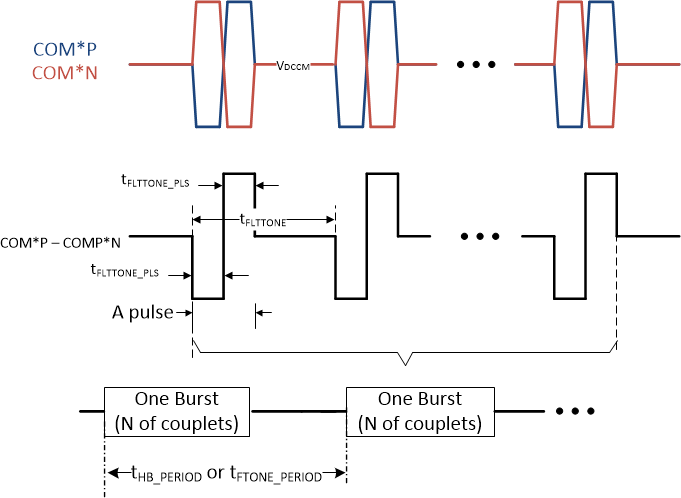
Other than data, certain information is transmitted using tone: signals to change power state of stack device (SLP2ACT tone, WAKE tone, SHUTDOWN tone, HWRST tone), signals related to faults (FAULT tone and HEARTBEAT tone). The definition of each tone is defined in Figure 7-22 and Figure 7-21.

Device can transmit and receive tones in summary below:

Table 7-7 Available Tones to BQ79600-Q1
DIRECTION NAME
Receive FAULT tone and HEARTBEAT tone
Transmit SLP2ACT tone, WAKE tone, SHUTDOWN tone, HWRST tone, HEARTBEAT tone

Note:

  • Device does not transmit Fault Tone as it uses Section 7.3.3.2.1 to signal fault if enabled.
  • SLP2ACT/WAKE/SHUTDOWN/HWRST tone transmitting is on demand when corresponding bit in register CONTROL1 and CONTROL2 is set.
  • When bridge device in SHUTDOWN, wakeup bridge device doesn’t change power mode of stack devices.
  • Receiving threshold value is defined as nHBDET, nFTONEDET in section 6.6.
  • Transmitting number is predefined by device in Table 7-8.

Table 7-8 Transmitting Tones Summary Table
SLP2ACT WAKE SHUTDOWN HWRST HEARTBEAT (SLEEP only)
N of Couplets Transmitted in Single Burst 30 90 270 810 30
Burst Period NA NA NA NA 400ms
GUID-96F28D8D-788C-4224-A3F3-38022819FCD7-low.gif Figure 7-21 FAULT Tone and HEARTBEAT Tone Definition
GUID-4037620F-E590-4FBA-B96F-6A8F42CCEF95-low.gif Figure 7-22 SHUTDOWN, HEARTBEAT, HWRST, SLP2ACT Tone Definition