ZHCSQT5 July 2022 TPS7A57
PRODUCTION DATA
- 1 特性
- 2 应用
- 3 说明
- 4 Revision History
- 5 Pin Configuration and Functions
- 6 Specifications
-
7 Detailed Description
- 7.1 Overview
- 7.2 Functional Block Diagram
- 7.3
Feature Description
- 7.3.1 Output Voltage Setting and Regulation
- 7.3.2 Low-Noise, Ultra-High Power-Supply Rejection Ratio (PSRR)
- 7.3.3 Programmable Soft-Start (NR/SS Pin)
- 7.3.4 Precision Enable and UVLO
- 7.3.5 Charge Pump Enable and BIAS Rail
- 7.3.6 Power-Good Pin (PG Pin)
- 7.3.7 Active Discharge
- 7.3.8 Thermal Shutdown Protection (TSD)
- 7.4 Device Functional Modes
-
8 Application and Implementation
- 8.1
Application Information
- 8.1.1 Precision Enable (External UVLO)
- 8.1.2 Undervoltage Lockout (UVLO) Operation
- 8.1.3 Dropout Voltage (VDO)
- 8.1.4 Input and Output Capacitor Requirements (CIN and COUT)
- 8.1.5 Recommended Capacitor Types
- 8.1.6 Soft-Start, Noise Reduction (NR/SS Pin), and Power-Good (PG Pin)
- 8.1.7 Optimizing Noise and PSRR
- 8.1.8 Adjustable Operation
- 8.1.9 Load Transient Response
- 8.1.10 Current Limit and Foldback Behavior
- 8.1.11 Charge Pump Operation
- 8.1.12 Sequencing
- 8.1.13 Power-Good Functionality
- 8.1.14 Output Impedance
- 8.1.15 Paralleling for Higher Output Current and Lower Noise
- 8.1.16 Current Mode Margining
- 8.1.17 Voltage Mode Margining
- 8.1.18 Power Dissipation (PD)
- 8.1.19 Estimating Junction Temperature
- 8.1.20 TPS7A57EVM-081 Thermal Analysis
- 8.2 Typical Application
- 8.3 Power Supply Recommendations
- 8.4 Layout
- 8.1
Application Information
- 9 Device and Documentation Support
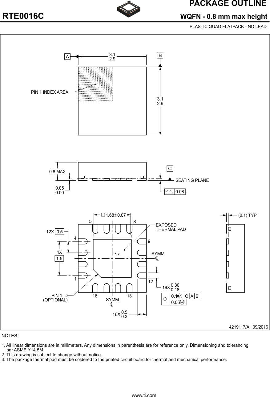
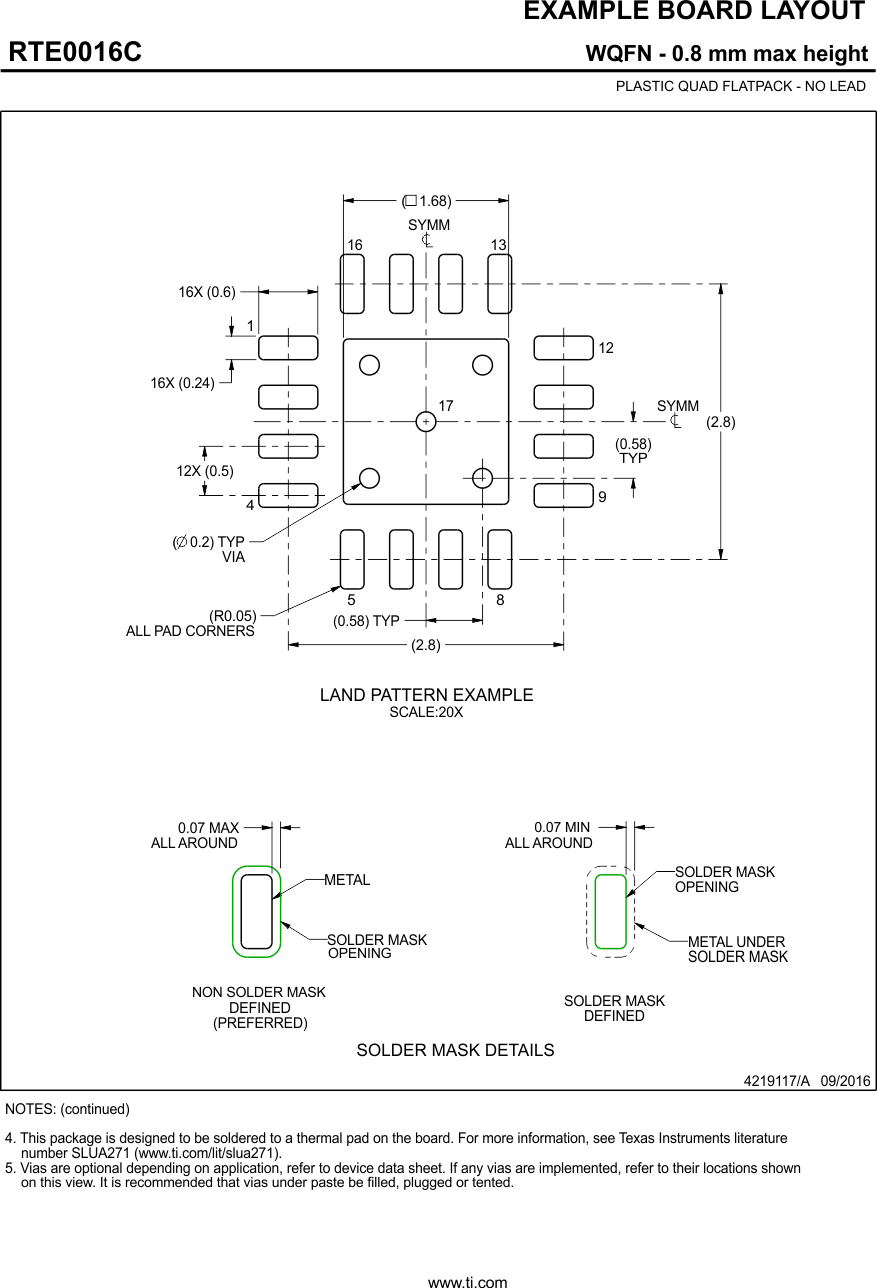
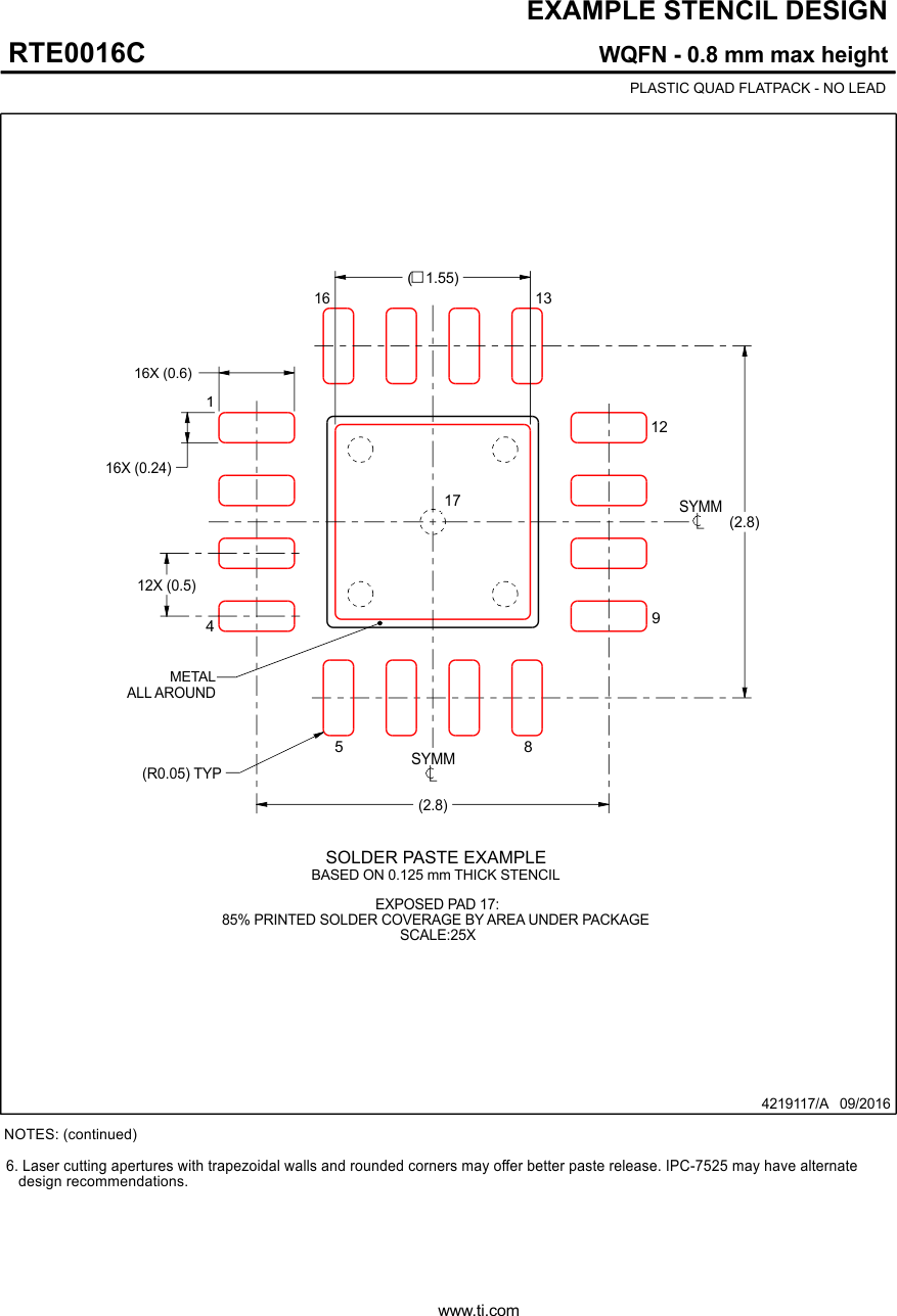
- 10Mechanical, Packaging, and Orderable Information
10.1 Mechanical Data


