ZHCSQT5 July 2022 TPS7A57
PRODUCTION DATA
- 1 特性
- 2 应用
- 3 说明
- 4 Revision History
- 5 Pin Configuration and Functions
- 6 Specifications
-
7 Detailed Description
- 7.1 Overview
- 7.2 Functional Block Diagram
- 7.3
Feature Description
- 7.3.1 Output Voltage Setting and Regulation
- 7.3.2 Low-Noise, Ultra-High Power-Supply Rejection Ratio (PSRR)
- 7.3.3 Programmable Soft-Start (NR/SS Pin)
- 7.3.4 Precision Enable and UVLO
- 7.3.5 Charge Pump Enable and BIAS Rail
- 7.3.6 Power-Good Pin (PG Pin)
- 7.3.7 Active Discharge
- 7.3.8 Thermal Shutdown Protection (TSD)
- 7.4 Device Functional Modes
-
8 Application and Implementation
- 8.1
Application Information
- 8.1.1 Precision Enable (External UVLO)
- 8.1.2 Undervoltage Lockout (UVLO) Operation
- 8.1.3 Dropout Voltage (VDO)
- 8.1.4 Input and Output Capacitor Requirements (CIN and COUT)
- 8.1.5 Recommended Capacitor Types
- 8.1.6 Soft-Start, Noise Reduction (NR/SS Pin), and Power-Good (PG Pin)
- 8.1.7 Optimizing Noise and PSRR
- 8.1.8 Adjustable Operation
- 8.1.9 Load Transient Response
- 8.1.10 Current Limit and Foldback Behavior
- 8.1.11 Charge Pump Operation
- 8.1.12 Sequencing
- 8.1.13 Power-Good Functionality
- 8.1.14 Output Impedance
- 8.1.15 Paralleling for Higher Output Current and Lower Noise
- 8.1.16 Current Mode Margining
- 8.1.17 Voltage Mode Margining
- 8.1.18 Power Dissipation (PD)
- 8.1.19 Estimating Junction Temperature
- 8.1.20 TPS7A57EVM-081 Thermal Analysis
- 8.2 Typical Application
- 8.3 Power Supply Recommendations
- 8.4 Layout
- 8.1
Application Information
- 9 Device and Documentation Support
- 10Mechanical, Packaging, and Orderable Information
8.1.17 Voltage Mode Margining
Output voltage margining is a technique that allows a circuit to be evaluated for how well changes are tolerated in the power supply. This test is typically performed by adjusting the supply voltage to a fixed percentage above and below its nominal output voltage.
This section discusses the implementation of a voltage mode margining application using the TPS7A57. A margining target of ±5% is used to demonstrate the chosen implementation.
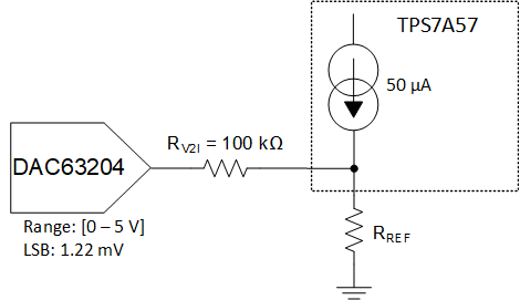
Figure 8-26 shows a simplified visualization of the TPS7A57 REF pin with a voltage DAC.
 Figure 8-26 Simplified Voltage Mode
Margining Schematic
Figure 8-26 Simplified Voltage Mode
Margining SchematicTable 8-7 summarizes the design requirements.
| PARAMETER | DESIGN VALUES |
|---|---|
| VIN | 2.5 V |
| VOUT | 1.8 V nominal with ±5% margining |
| CNR/SS | 4.7 μF |
| RREF | 36 kΩ |
| DAC VOUT range | 1.432 V to 2.108 V |
In this example, the output voltage is set to a nominal 1.8-V using a 36-kΩ resistor at the REF pin to GND. Equation 12 calculates the value for the RREF resistor.
The DAC63204, a 4-channel, 12-bit voltage and current output DAC with I2C, was selected and programmed into the voltage-output mode with an output range set between 1.432 V and 2.108 V. In conjunction with the 12-bit voltage DAC resolution, this output range allows a minimum step size (or LSB) of approximately 1.22 mV or 122 μA when the voltage-to-input (V2I) conversion or RV2I (100 kΩ) is taken into consideration. Into the 36-kΩ resistor, this LSB translates into a 0.44-mV voltage resolution or approximately 0.025% of the nominal 1.8-V targeted voltage. To achieve the full ±5% swing around the nominal voltage, the DAC63204 must source 3.1 μA or sink 3.7 μA.
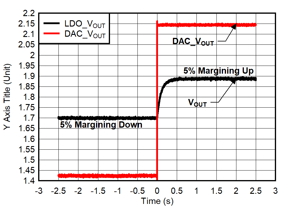
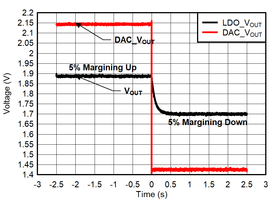
The current flowing through RREF changes to 53.1 μA and 46.3 μA, thus adjusting the output voltage to 1.88 V and 1.7 V respectively.
Section 8.1.17 and Figure 8-28 show the voltage margining results.
 Figure 8-27 Margining From –5% to
+5%
 Figure 8-28 Margining from +5% to
–5%
Figure 8-28 Margining from +5% to
–5%When implementing voltage margining with this LDO, there is a time constant associated with its response. This RC time constant originates from the parallel combination of RREF and CNR/SS. Section 8.1.17 and Figure 8-28 show this RC effect.
Equation 13 calculates the time constant for this implementation:
where:
- RREF is 36 kΩ
- CNR/SS is 4.7 μF
- τ = 169 ms