ZHCSQT5 July 2022 TPS7A57
PRODUCTION DATA
- 1 特性
- 2 应用
- 3 说明
- 4 Revision History
- 5 Pin Configuration and Functions
- 6 Specifications
-
7 Detailed Description
- 7.1 Overview
- 7.2 Functional Block Diagram
- 7.3
Feature Description
- 7.3.1 Output Voltage Setting and Regulation
- 7.3.2 Low-Noise, Ultra-High Power-Supply Rejection Ratio (PSRR)
- 7.3.3 Programmable Soft-Start (NR/SS Pin)
- 7.3.4 Precision Enable and UVLO
- 7.3.5 Charge Pump Enable and BIAS Rail
- 7.3.6 Power-Good Pin (PG Pin)
- 7.3.7 Active Discharge
- 7.3.8 Thermal Shutdown Protection (TSD)
- 7.4 Device Functional Modes
-
8 Application and Implementation
- 8.1
Application Information
- 8.1.1 Precision Enable (External UVLO)
- 8.1.2 Undervoltage Lockout (UVLO) Operation
- 8.1.3 Dropout Voltage (VDO)
- 8.1.4 Input and Output Capacitor Requirements (CIN and COUT)
- 8.1.5 Recommended Capacitor Types
- 8.1.6 Soft-Start, Noise Reduction (NR/SS Pin), and Power-Good (PG Pin)
- 8.1.7 Optimizing Noise and PSRR
- 8.1.8 Adjustable Operation
- 8.1.9 Load Transient Response
- 8.1.10 Current Limit and Foldback Behavior
- 8.1.11 Charge Pump Operation
- 8.1.12 Sequencing
- 8.1.13 Power-Good Functionality
- 8.1.14 Output Impedance
- 8.1.15 Paralleling for Higher Output Current and Lower Noise
- 8.1.16 Current Mode Margining
- 8.1.17 Voltage Mode Margining
- 8.1.18 Power Dissipation (PD)
- 8.1.19 Estimating Junction Temperature
- 8.1.20 TPS7A57EVM-081 Thermal Analysis
- 8.2 Typical Application
- 8.3 Power Supply Recommendations
- 8.4 Layout
- 8.1
Application Information
- 9 Device and Documentation Support
- 10Mechanical, Packaging, and Orderable Information
8.1.19 Estimating Junction Temperature
The JEDEC standard now recommends the use of psi (Ψ) thermal metrics to estimate the junction temperatures of the LDO when in-circuit on a typical PCB board application. These metrics are not strictly speaking thermal resistances, but rather offer practical and relative means of estimating junction temperatures. These psi metrics are determined to be significantly independent of the copper-spreading area. The key thermal metrics (ΨJT and ΨJB) are used in accordance with Equation 17 and are given in the Section 6.5 table.
Equation 17. 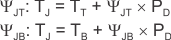
where:
- PD is the power dissipated as explained in Equation 14
- TT is the temperature at the center-top of the device package
- TB is the PCB surface temperature measured 1 mm from the device package and centered on the package edge