ZHCSQT5 July 2022 TPS7A57
PRODUCTION DATA
- 1 特性
- 2 应用
- 3 说明
- 4 Revision History
- 5 Pin Configuration and Functions
- 6 Specifications
-
7 Detailed Description
- 7.1 Overview
- 7.2 Functional Block Diagram
- 7.3
Feature Description
- 7.3.1 Output Voltage Setting and Regulation
- 7.3.2 Low-Noise, Ultra-High Power-Supply Rejection Ratio (PSRR)
- 7.3.3 Programmable Soft-Start (NR/SS Pin)
- 7.3.4 Precision Enable and UVLO
- 7.3.5 Charge Pump Enable and BIAS Rail
- 7.3.6 Power-Good Pin (PG Pin)
- 7.3.7 Active Discharge
- 7.3.8 Thermal Shutdown Protection (TSD)
- 7.4 Device Functional Modes
-
8 Application and Implementation
- 8.1
Application Information
- 8.1.1 Precision Enable (External UVLO)
- 8.1.2 Undervoltage Lockout (UVLO) Operation
- 8.1.3 Dropout Voltage (VDO)
- 8.1.4 Input and Output Capacitor Requirements (CIN and COUT)
- 8.1.5 Recommended Capacitor Types
- 8.1.6 Soft-Start, Noise Reduction (NR/SS Pin), and Power-Good (PG Pin)
- 8.1.7 Optimizing Noise and PSRR
- 8.1.8 Adjustable Operation
- 8.1.9 Load Transient Response
- 8.1.10 Current Limit and Foldback Behavior
- 8.1.11 Charge Pump Operation
- 8.1.12 Sequencing
- 8.1.13 Power-Good Functionality
- 8.1.14 Output Impedance
- 8.1.15 Paralleling for Higher Output Current and Lower Noise
- 8.1.16 Current Mode Margining
- 8.1.17 Voltage Mode Margining
- 8.1.18 Power Dissipation (PD)
- 8.1.19 Estimating Junction Temperature
- 8.1.20 TPS7A57EVM-081 Thermal Analysis
- 8.2 Typical Application
- 8.3 Power Supply Recommendations
- 8.4 Layout
- 8.1
Application Information
- 9 Device and Documentation Support
- 10Mechanical, Packaging, and Orderable Information
8.1.15 Paralleling for Higher Output Current and Lower Noise
Achieving higher output current and lower noise is achievable by paralleling two or more LDOs. Implementation must be carefully planned out to optimize performance and minimize output current imbalance.
Because the TPS7A57 output voltage is set by a resistor driven by a current source, the REF resistor and capacitor must be adjusted as per the following:
where:
- n is the number of LDOs in parallel
- IREF is the REF current as provided in the Section 6.5 table
- CNR/SS_single is the NR/SS capacitor for a single LDO. Note that each LDO must have its own CNR/SS capacitor.
When connecting the IN pins together, and with the LDO being a buffer, the current imbalance is only affected by the error offset voltage of the error amplifier. As such, the current imbalance can be expressed as:
where:
- εI is the current imbalance
- VOS is the LDO error offset voltage
- RBALLAST is the ballast resistor
- ΔRBALLAST is the deviation of the ballast resistor value from the nominal value
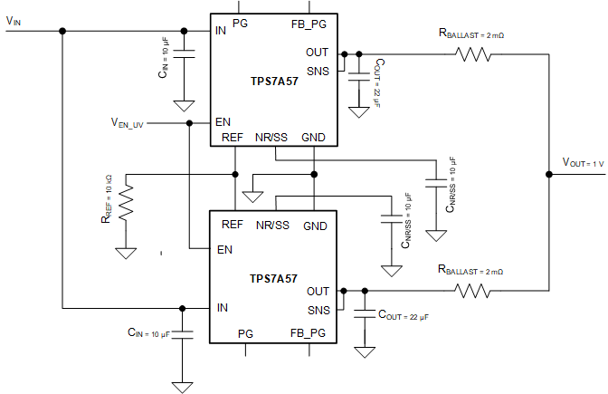
With the typical offset voltage of 200 μV, the ballast resistor must be 2 mΩ or greater (as shown in Figure 8-22), considering no error from the design of the PCB ballast resistor (ΔRBALLAST = 0 Ω) and a 100-mA maximum current imbalance.
 Figure 8-22 Paralleling Multiple TPS7A57
Devices
Figure 8-22 Paralleling Multiple TPS7A57
DevicesUsing the configuration described, the LDO output noise is reduced by:
where:
- n is the numbers of LDOs in parallel
- eO_single is the output noise density from a single LDO
- eO_parallel is the output noise density for the resulting parallel LDO
In Figure 8-22, the noise is reduced by 1/√2.