ZHCSB89H May   2013  – December 2021 TPS65310A-Q1

PRODUCTION DATA  

  1. 特性
  2. 应用
  3. 说明
  4. Revision History
  5. 说明(续)
  6. Pin Configuration and Functions
  7. Specifications
    1. 7.1 Absolute Maximum Ratings
    2. 7.2 ESD Ratings
    3. 7.3 Recommended Operating Conditions
    4. 7.4 Thermal Information
    5. 7.5 Electrical Characteristics
    6. 7.6 SPI Timing Requirements
    7. 7.7 Typical Characteristics
  8. Detailed Description
    1. 8.1 Overview
    2. 8.2 Functional Block Diagram
    3. 8.3 Feature Description
      1. 8.3.1 Buck Controller (Buck1)
        1. 8.3.1.1 Operating Modes
        2. 8.3.1.2 Normal Mode PWM Operation
      2. 8.3.2 Synchronous Buck Converters Buck2 And Buck3
      3. 8.3.3 BOOST Converter
      4. 8.3.4 Frequency-Hopping Spread Spectrum
      5. 8.3.5 Linear Regulator LDO
      6. 8.3.6 Gate Driver Supply
    4. 8.4 Device Functional Modes
      1. 8.4.1  RESET
      2. 8.4.2  Soft Start
      3. 8.4.3  INIT
      4. 8.4.4  TESTSTART
      5. 8.4.5  TESTSTOP
      6. 8.4.6  VTCHECK
      7. 8.4.7  RAMP
      8. 8.4.8  Power-Up Sequencing
      9. 8.4.9  Power-Down Sequencing
      10. 8.4.10 Active
      11. 8.4.11 ERROR
      12. 8.4.12 LOCKED
      13. 8.4.13 LPM0
      14. 8.4.14 Shutdown
        1. 8.4.14.1 Power-On Reset Flag
      15. 8.4.15 Wake Pin
      16. 8.4.16 IRQ Pin
      17. 8.4.17 VBAT Undervoltage Warning
      18. 8.4.18 VIN Over Or Undervoltage Protection
      19. 8.4.19 External Protection
      20. 8.4.20 Overtemperature Detection And Shutdown
      21. 8.4.21 Independent Voltage Monitoring
      22. 8.4.22 GND Loss Detection
      23. 8.4.23 Reference Voltage
      24. 8.4.24 Shutdown Comparator
      25. 8.4.25 LED And High-Side Switch Control
      26. 8.4.26 Window Watchdog
      27. 8.4.27 Timeout In Start-Up Modes
    5. 8.5 Programming
      1. 8.5.1 SPI
        1. 8.5.1.1 FSI Bit
    6. 8.6 Register Maps
      1. 8.6.1 Register Description
      2. 8.6.2 NOP0X00
        1. 8.6.2.1  SPI_SCK_FAIL 0x03
        2. 8.6.2.2  LPMO_CMD 0x11
        3. 8.6.2.3  LOCK_CMD 0x12
        4. 8.6.2.4  PWR_STAT 0x21
        5. 8.6.2.5  SYS_STAT 0x22
        6. 8.6.2.6  SPI_STAT 0x23
        7. 8.6.2.7  COMP_STAT 0x24
        8. 8.6.2.8  DEV_REV 0x2F
        9. 8.6.2.9  PWR_CONFIG 0x31
        10. 8.6.2.10 DEV_CONFIG 0x32
        11. 8.6.2.11 CLOCK_CONFIG 0x33
  9. Application and Implementation
    1. 9.1 Application Information
    2. 9.2 Typical Applications
      1. 9.2.1 Buck Controller 1
        1. 9.2.1.1 Design Requirements
        2. 9.2.1.2 Detailed Design Procedure
          1. 9.2.1.2.1 Adjusting the Output Voltage for the BUCK1 Controller
          2. 9.2.1.2.2 Output Inductor, Sense Resistor and Capacitor Selection for the BUCK1 Controller
          3. 9.2.1.2.3 Compensation of the Buck Controller
          4. 9.2.1.2.4 Bootstrap Capacitor for the BUCK1 Controller
        3. 9.2.1.3 BUCK 1 Application Curve
      2. 9.2.2 Synchronous Buck Converters BUCK2 and BUCK3
        1. 9.2.2.1 Design Requirements
        2. 9.2.2.2 Detailed Design Procedure
          1. 9.2.2.2.1 Adjusting the Output Voltage for the BUCK2 and BUCK3 Converter
          2. 9.2.2.2.2 Output Inductor Selection for the BUCK2 and BUCK3 Converter
          3. 9.2.2.2.3 Compensation of the BUCK2 and BUCK3 Converters
          4. 9.2.2.2.4 Bootstrap Capacitor for the BUCK2/3 Converters
        3. 9.2.2.3 Application Curves
      3. 9.2.3 BOOST Converter
        1. 9.2.3.1 Design Requirements
        2. 9.2.3.2 Detailed Design Procedure
          1. 9.2.3.2.1 Adjusting the Output Voltage for the Boost Converter
          2. 9.2.3.2.2 Output Inductor and Capacitor Selection for the BOOST Converter
          3. 9.2.3.2.3 Compensation of the BOOST Converter
          4. 9.2.3.2.4 Output Diode for the BOOST Converter
        3. 9.2.3.3 BOOST Converter Application Curves
      4. 9.2.4 Linear Regulator
        1. 9.2.4.1 Design Requirements
        2. 9.2.4.2 Detailed Design Procedure
          1. 9.2.4.2.1 Adjusting the Output Voltage for the Linear Regulator
          2. 9.2.4.2.2 Output Capacitance for the Linear Regulator
        3. 9.2.4.3 Linear Regulator Application Curve
  10. 10Power Supply Recommendations
  11. 11Layout
    1. 11.1 Layout Guidelines
      1. 11.1.1 Buck Controller
      2. 11.1.2 Buck Converter
      3. 11.1.3 Boost Converter
      4. 11.1.4 Linear Regulator
      5. 11.1.5 Other Considerations
    2. 11.2 Layout Example
  12. 12Device and Documentation Support
    1. 12.1 Documentation Support
      1. 12.1.1 Related Documentation
    2. 12.2 接收文档更新通知
    3. 12.3 支持资源
    4. 12.4 Trademarks
    5. 12.5 Electrostatic Discharge Caution
    6. 12.6 术语表
  13. 13Mechanical, Packaging, and Orderable Information

封装选项

机械数据 (封装 | 引脚)
散热焊盘机械数据 (封装 | 引脚)
订购信息

Power Supply Recommendations

The device is designed to operate from an input voltage supply range between 4 V and 40 V (see Figure 10-1 for reference). This input supply must be well regulated. In case the supply voltage in the application is likely to exceed 40 V, the external PMOS protection device as explained in Section 8.4.19 must be applied between VIN and VINPROT pins. Furthermore, if the supply voltage in the application is likely to reach negative voltage (for example, reverse battery), a forward diode must be placed between the VSSENSE and VIN pins. A ceramic bypass capacitor with a value of 100 μF (typical) is recommended to be placed close to the VINPROT pin. For the VIN pin, a small ceramic capacitor of typical 1 µF is recommended. Also place 1-µF (typical) bypass capacitors to the DVDD and VREF pins, and 100-nF (typical) bypass capacitors to VIO pin. Furthermore, the VREG pin requires a bypass capacitor of 2.2 µF (typical).

The BUCK1 output voltage is the recommended input supply for the BUCK2, BUCK3, and BOOST regulators. Place local, 10-µF (typical) bypass capacitors at the VSUP2 and VSUP3 pins and at the supply input of the BOOST in front of the BOOST-inductor. Also place a local, 1-µF (typical) bypass capacitor at the VSUP4 pin.

The EXTSUP pin can be used to improve efficiency. For the EXTSUP pin to improve efficiency, a voltage of more than 4.8 V is required in order to have VREG regulator supplied from EXTSUP pin. If the EXSUP pin is not used, the VINPROT pin supplies the VREG regulator. The EXTSUP pin requires a 100-nF (typical) bypass capacitor.
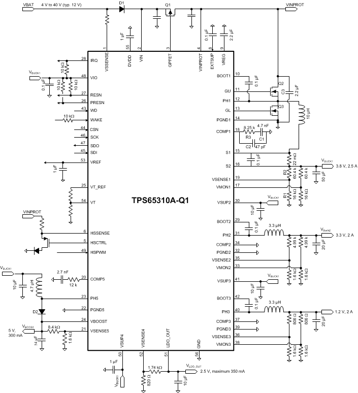
GUID-77CD2DD3-E91E-45DF-87DD-100F157E5DAD-low.gif Figure 10-1 Typical Application Schematic