ZHCSB89H May 2013 – December 2021 TPS65310A-Q1
PRODUCTION DATA
- 1 特性
- 2 应用
- 3 说明
- 4 Revision History
- 5 说明(续)
- 6 Pin Configuration and Functions
- 7 Specifications
-
8 Detailed Description
- 8.1 Overview
- 8.2 Functional Block Diagram
- 8.3 Feature Description
- 8.4
Device Functional Modes
- 8.4.1 RESET
- 8.4.2 Soft Start
- 8.4.3 INIT
- 8.4.4 TESTSTART
- 8.4.5 TESTSTOP
- 8.4.6 VTCHECK
- 8.4.7 RAMP
- 8.4.8 Power-Up Sequencing
- 8.4.9 Power-Down Sequencing
- 8.4.10 Active
- 8.4.11 ERROR
- 8.4.12 LOCKED
- 8.4.13 LPM0
- 8.4.14 Shutdown
- 8.4.15 Wake Pin
- 8.4.16 IRQ Pin
- 8.4.17 VBAT Undervoltage Warning
- 8.4.18 VIN Over Or Undervoltage Protection
- 8.4.19 External Protection
- 8.4.20 Overtemperature Detection And Shutdown
- 8.4.21 Independent Voltage Monitoring
- 8.4.22 GND Loss Detection
- 8.4.23 Reference Voltage
- 8.4.24 Shutdown Comparator
- 8.4.25 LED And High-Side Switch Control
- 8.4.26 Window Watchdog
- 8.4.27 Timeout In Start-Up Modes
- 8.5 Programming
- 8.6 Register Maps
-
9 Application and Implementation
- 9.1 Application Information
- 9.2
Typical Applications
- 9.2.1 Buck Controller 1
- 9.2.2 Synchronous Buck Converters BUCK2 and BUCK3
- 9.2.3 BOOST Converter
- 9.2.4 Linear Regulator
- 10Power Supply Recommendations
- 11Layout
- 12Device and Documentation Support
- 13Mechanical, Packaging, and Orderable Information
8.4.1 RESET
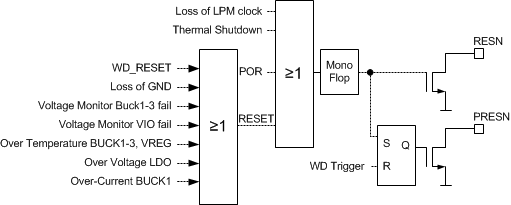
RESN and PRESN are open drain outputs which are active if one or more of the conditions listed in Table 8-1 are valid. RESN active (low) is extended for tRESNHOLD after a reset is triggered. RESN is the main processor reset and also asserts PRESN as a peripheral signal.
PRESN is latched and is released when window trigger mode of the watchdog is enabled (first rising edge at WD pin).
RESN and PRESN must keep the main processor and peripheral devices in a defined state during power up and power down in case of improper supply voltages or a critical failure condition. Therefore, for low supply voltages the topology of the reset outputs specify that RESN and PRESN are always held at a low level when RESN and PRESN are asserted, even if VIN falls below VPOR or the device is in SHUTDOWN mode.
 Figure 8-3 RESET Functionality
| RESET CONDITIONS | |
|---|---|
| POR, Loss of LPM Clock, and Thermal Shutdown | The device reinitializes all registers with their default values. Error counter is cleared. |
| Voltage Monitor BUCK 1-3 | Input voltage at VMON1-3 pin out-of-bounds: VVMON1-3 < VMONTH_L or VVMON1-3 > VMONTH_H |
| Over Voltage LDO | Vsense4 > VMONTH_H |
| Voltage Monitor VIO | Input voltage at VIO pin out-of-bounds: VVIO < VVIOMON TH |
| Loss of GND | Open at PGNDx or GND pin |
| OT BUCK1-3, VREG | Overtemperature on BUCK1–3 or VREG |
| WD_RESET | Watchdog window violation |
Any reset event (without POR, thermal shutdown, or loss of LPM clock) increments the error counter (EC) by one. After a reset is consecutively triggered NRES times, the device transfers to the LPM0 state, and the EC is reset to 0. The counter is decremented by one if an SPI LPM0_CMD is received. Alternatively, the device can be put in LOCK state once an SPI LOCK_CMD is received. Once the device is locked, it cannot be activated again by a wake condition. The reset counter and lock function avoid cyclic start-up and shut-down of the device in case of a persistent fault condition. The reset counter content is cleared with a POR condition, a thermal shutdown or a loss of LPM clock. Once the device is locked, a voltage below VPOR at the VIN pin or a thermal shutdown condition are the only ways to unlock the device.