ZHCSB89H May   2013  – December 2021 TPS65310A-Q1

PRODUCTION DATA  

  1. 特性
  2. 应用
  3. 说明
  4. Revision History
  5. 说明(续)
  6. Pin Configuration and Functions
  7. Specifications
    1. 7.1 Absolute Maximum Ratings
    2. 7.2 ESD Ratings
    3. 7.3 Recommended Operating Conditions
    4. 7.4 Thermal Information
    5. 7.5 Electrical Characteristics
    6. 7.6 SPI Timing Requirements
    7. 7.7 Typical Characteristics
  8. Detailed Description
    1. 8.1 Overview
    2. 8.2 Functional Block Diagram
    3. 8.3 Feature Description
      1. 8.3.1 Buck Controller (Buck1)
        1. 8.3.1.1 Operating Modes
        2. 8.3.1.2 Normal Mode PWM Operation
      2. 8.3.2 Synchronous Buck Converters Buck2 And Buck3
      3. 8.3.3 BOOST Converter
      4. 8.3.4 Frequency-Hopping Spread Spectrum
      5. 8.3.5 Linear Regulator LDO
      6. 8.3.6 Gate Driver Supply
    4. 8.4 Device Functional Modes
      1. 8.4.1  RESET
      2. 8.4.2  Soft Start
      3. 8.4.3  INIT
      4. 8.4.4  TESTSTART
      5. 8.4.5  TESTSTOP
      6. 8.4.6  VTCHECK
      7. 8.4.7  RAMP
      8. 8.4.8  Power-Up Sequencing
      9. 8.4.9  Power-Down Sequencing
      10. 8.4.10 Active
      11. 8.4.11 ERROR
      12. 8.4.12 LOCKED
      13. 8.4.13 LPM0
      14. 8.4.14 Shutdown
        1. 8.4.14.1 Power-On Reset Flag
      15. 8.4.15 Wake Pin
      16. 8.4.16 IRQ Pin
      17. 8.4.17 VBAT Undervoltage Warning
      18. 8.4.18 VIN Over Or Undervoltage Protection
      19. 8.4.19 External Protection
      20. 8.4.20 Overtemperature Detection And Shutdown
      21. 8.4.21 Independent Voltage Monitoring
      22. 8.4.22 GND Loss Detection
      23. 8.4.23 Reference Voltage
      24. 8.4.24 Shutdown Comparator
      25. 8.4.25 LED And High-Side Switch Control
      26. 8.4.26 Window Watchdog
      27. 8.4.27 Timeout In Start-Up Modes
    5. 8.5 Programming
      1. 8.5.1 SPI
        1. 8.5.1.1 FSI Bit
    6. 8.6 Register Maps
      1. 8.6.1 Register Description
      2. 8.6.2 NOP0X00
        1. 8.6.2.1  SPI_SCK_FAIL 0x03
        2. 8.6.2.2  LPMO_CMD 0x11
        3. 8.6.2.3  LOCK_CMD 0x12
        4. 8.6.2.4  PWR_STAT 0x21
        5. 8.6.2.5  SYS_STAT 0x22
        6. 8.6.2.6  SPI_STAT 0x23
        7. 8.6.2.7  COMP_STAT 0x24
        8. 8.6.2.8  DEV_REV 0x2F
        9. 8.6.2.9  PWR_CONFIG 0x31
        10. 8.6.2.10 DEV_CONFIG 0x32
        11. 8.6.2.11 CLOCK_CONFIG 0x33
  9. Application and Implementation
    1. 9.1 Application Information
    2. 9.2 Typical Applications
      1. 9.2.1 Buck Controller 1
        1. 9.2.1.1 Design Requirements
        2. 9.2.1.2 Detailed Design Procedure
          1. 9.2.1.2.1 Adjusting the Output Voltage for the BUCK1 Controller
          2. 9.2.1.2.2 Output Inductor, Sense Resistor and Capacitor Selection for the BUCK1 Controller
          3. 9.2.1.2.3 Compensation of the Buck Controller
          4. 9.2.1.2.4 Bootstrap Capacitor for the BUCK1 Controller
        3. 9.2.1.3 BUCK 1 Application Curve
      2. 9.2.2 Synchronous Buck Converters BUCK2 and BUCK3
        1. 9.2.2.1 Design Requirements
        2. 9.2.2.2 Detailed Design Procedure
          1. 9.2.2.2.1 Adjusting the Output Voltage for the BUCK2 and BUCK3 Converter
          2. 9.2.2.2.2 Output Inductor Selection for the BUCK2 and BUCK3 Converter
          3. 9.2.2.2.3 Compensation of the BUCK2 and BUCK3 Converters
          4. 9.2.2.2.4 Bootstrap Capacitor for the BUCK2/3 Converters
        3. 9.2.2.3 Application Curves
      3. 9.2.3 BOOST Converter
        1. 9.2.3.1 Design Requirements
        2. 9.2.3.2 Detailed Design Procedure
          1. 9.2.3.2.1 Adjusting the Output Voltage for the Boost Converter
          2. 9.2.3.2.2 Output Inductor and Capacitor Selection for the BOOST Converter
          3. 9.2.3.2.3 Compensation of the BOOST Converter
          4. 9.2.3.2.4 Output Diode for the BOOST Converter
        3. 9.2.3.3 BOOST Converter Application Curves
      4. 9.2.4 Linear Regulator
        1. 9.2.4.1 Design Requirements
        2. 9.2.4.2 Detailed Design Procedure
          1. 9.2.4.2.1 Adjusting the Output Voltage for the Linear Regulator
          2. 9.2.4.2.2 Output Capacitance for the Linear Regulator
        3. 9.2.4.3 Linear Regulator Application Curve
  10. 10Power Supply Recommendations
  11. 11Layout
    1. 11.1 Layout Guidelines
      1. 11.1.1 Buck Controller
      2. 11.1.2 Buck Converter
      3. 11.1.3 Boost Converter
      4. 11.1.4 Linear Regulator
      5. 11.1.5 Other Considerations
    2. 11.2 Layout Example
  12. 12Device and Documentation Support
    1. 12.1 Documentation Support
      1. 12.1.1 Related Documentation
    2. 12.2 接收文档更新通知
    3. 12.3 支持资源
    4. 12.4 Trademarks
    5. 12.5 Electrostatic Discharge Caution
    6. 12.6 术语表
  13. 13Mechanical, Packaging, and Orderable Information

封装选项

机械数据 (封装 | 引脚)
散热焊盘机械数据 (封装 | 引脚)
订购信息

LED And High-Side Switch Control

This module controls an external PMOS in current-limited high-side switch.

The current levels can be adjusted with an external sense resistor. Enable and disable is done with the HS_EN bit. The switch is controlled by the HSPWM input pin. Driving HSPWM high turns on the external FET.

The device offers an open load diagnostic indicated by the HS_OL flag in the SPI register PWR_STAT. Open load is also indicated in case the voltage on VINPROT–VSSENSE does not drop below the threshold when PWM is low (self-test).

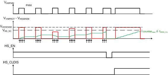
A counter monitors the overcurrent condition to detect the risk of overheating. While HSPWM = high and HS_EN = high the counter is incremented during overcurrent conditions, and decremented if the current is below the overcurrent threshold at a sampling interval of tS HS (shown in Figure 8-9). When reaching a net current limit time of tHSS CL, the driver is turned off and the HS_EN bit is cleared. This feature can be disabled by SPI bit HS_CLDIS. When HS_EN is cleared, the counter is reset.
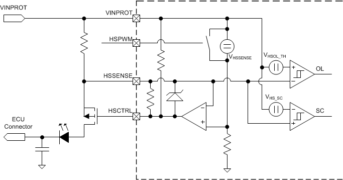
GUID-A253AC65-000F-41BD-B8EB-7CCADCB564E5-low.gif Figure 8-8 High-Side Control Circuit
GUID-5EFC0144-7F6F-493C-9FA2-BD9A313F1B35-low.gif Figure 8-9 HS Overcurrent Counter
Note:

In case the LED or High-Side Switch Control is not used in the application, HSSENSE must be connected to VINPROT