SPRS357D August   2006  – June 2020 TMS320F28044

PRODUCTION DATA.  

  1. 1Device Overview
    1. 1.1 Features
    2. 1.2 Applications
    3. 1.3 Description
    4. 1.4 Functional Block Diagram
  2. 2Revision History
  3. 3Device Comparison
    1. 3.1 Related Products
  4. 4Terminal Configuration and Functions
    1. 4.1 Pin Diagrams
    2. 4.2 Signal Descriptions
  5. 5Specifications
    1. 5.1  Absolute Maximum Ratings
    2. 5.2  ESD Ratings – Commercial
    3. 5.3  Recommended Operating Conditions
    4. 5.4  Power Consumption Summary
      1. Table 5-1 TMS320F28044 Current Consumption by Power-Supply Pins at 100-MHz SYSCLKOUT
      2. 5.4.1     Reducing Current Consumption
    5. 5.5  Electrical Characteristics
    6. 5.6  Thermal Resistance Characteristics for F28044 100-Ball GGM Package
    7. 5.7  Thermal Resistance Characteristics for F28044 100-Pin PZ Package
    8. 5.8  Thermal Design Considerations
    9. 5.9  Timing and Switching Characteristics
      1. 5.9.1 Timing Parameter Symbology
        1. 5.9.1.1 General Notes on Timing Parameters
        2. 5.9.1.2 Test Load Circuit
        3. 5.9.1.3 Device Clock Table
          1. Table 5-3 TMS320x280x Clock Table and Nomenclature
      2. 5.9.2 Power Sequencing
        1. 5.9.2.1   Power Management and Supervisory Circuit Solutions
        2. Table 5-5 Reset (XRS) Timing Requirements
      3. 5.9.3 Clock Requirements and Characteristics
        1. Table 5-6 Input Clock Frequency
        2. Table 5-7 XCLKIN Timing Requirements - PLL Enabled
        3. Table 5-8 XCLKIN Timing Requirements - PLL Disabled
        4. Table 5-9 XCLKOUT Switching Characteristics (PLL Bypassed or Enabled)
      4. 5.9.4 Peripherals
        1. 5.9.4.1 General-Purpose Input/Output (GPIO)
          1. 5.9.4.1.1 GPIO - Output Timing
            1. Table 5-10 General-Purpose Output Switching Characteristics
          2. 5.9.4.1.2 GPIO - Input Timing
            1. Table 5-11 General-Purpose Input Timing Requirements
          3. 5.9.4.1.3 Sampling Window Width for Input Signals
          4. 5.9.4.1.4 Low-Power Mode Wakeup Timing
            1. Table 5-12 IDLE Mode Timing Requirements
            2. Table 5-13 IDLE Mode Switching Characteristics
            3. Table 5-14 STANDBY Mode Timing Requirements
            4. Table 5-15 STANDBY Mode Switching Characteristics
            5. Table 5-16 HALT Mode Timing Requirements
            6. Table 5-17 HALT Mode Switching Characteristics
        2. 5.9.4.2 Enhanced Control Peripherals
          1. 5.9.4.2.1 Enhanced Pulse Width Modulator (ePWM) Timing
            1. Table 5-18 ePWM Timing Requirements
            2. Table 5-19 ePWM Switching Characteristics
          2. 5.9.4.2.2 Trip-Zone Input Timing
            1. Table 5-20 Trip-Zone input Timing Requirements
          3. 5.9.4.2.3 High-Resolution PWM Timing
            1. Table 5-21 High Resolution PWM Characteristics at SYSCLKOUT = (60 - 100 MHz)
          4. 5.9.4.2.4 ADC Start-of-Conversion Timing
            1. Table 5-22 External ADC Start-of-Conversion Switching Characteristics
        3. 5.9.4.3 External Interrupt Timing
          1. Table 5-23 External Interrupt Timing Requirements
          2. Table 5-24 External Interrupt Switching Characteristics
        4. 5.9.4.4 I2C Electrical Specification and Timing
          1. Table 5-25 I2C Timing
        5. 5.9.4.5 Serial Peripheral Interface (SPI) Master Mode Timing
          1. Table 5-26 SPI Master Mode External Timing (Clock Phase = 0)
          2. Table 5-27 SPI Master Mode External Timing (Clock Phase = 1)
        6. 5.9.4.6 SPI Slave Mode Timing
          1. Table 5-28 SPI Slave Mode External Timing (Clock Phase = 0)
          2. Table 5-29 SPI Slave Mode External Timing (Clock Phase = 1)
      5. 5.9.5 JTAG Debug Probe Connection Without Signal Buffering for the DSP
      6. 5.9.6 Flash Timing
        1. Table 5-30 Flash Endurance for A Temperature Material
        2. Table 5-31 Flash Parameters at 100-MHz SYSCLKOUT
        3. Table 5-32 Flash/OTP Access Timing
        4. Table 5-33 Flash Data Retention Duration
    10. 5.10 On-Chip Analog-to-Digital Converter
      1. Table 5-35 ADC Electrical Characteristics (over recommended operating conditions)
      2. 5.10.1     ADC Power-Up Control Bit Timing
        1. Table 5-36 ADC Power-Up Delays
        2. Table 5-37 Current Consumption for Different ADC Configurations (at 25-MHz ADCCLK)
      3. 5.10.2     Definitions
      4. 5.10.3     Sequential Sampling Mode (Single-Channel) (SMODE = 0)
        1. Table 5-38 Sequential Sampling Mode Timing
      5. 5.10.4     Simultaneous Sampling Mode (Dual-Channel) (SMODE = 1)
        1. Table 5-39 Simultaneous Sampling Mode Timing
      6. 5.10.5     Detailed Descriptions
  6. 6Detailed Description
    1. 6.1 Brief Descriptions
      1. 6.1.1  C28x CPU
      2. 6.1.2  Memory Bus (Harvard Bus Architecture)
      3. 6.1.3  Peripheral Bus
      4. 6.1.4  Real-Time JTAG and Analysis
      5. 6.1.5  Flash
      6. 6.1.6  M0, M1 SARAMs
      7. 6.1.7  L0, L1 SARAMs
      8. 6.1.8  Boot ROM
      9. 6.1.9  Security
      10. 6.1.10 Peripheral Interrupt Expansion (PIE) Block
      11. 6.1.11 External Interrupts (XINT1, XINT2, XNMI)
      12. 6.1.12 Oscillator and PLL
      13. 6.1.13 Watchdog
      14. 6.1.14 Peripheral Clocking
      15. 6.1.15 Low-Power Modes
      16. 6.1.16 Peripheral Frames 0, 1, 2 (PFn)
      17. 6.1.17 General-Purpose Input/Output (GPIO) Multiplexer
      18. 6.1.18 32-Bit CPU-Timers (0, 1, 2)
      19. 6.1.19 Control Peripherals
      20. 6.1.20 Serial Port Peripherals
    2. 6.2 Peripherals
      1. 6.2.1 32-Bit CPU-Timers 0/1/2
      2. 6.2.2 Enhanced PWM Modules (ePWM1–16)
      3. 6.2.3 Hi-Resolution PWM (HRPWM)
      4. 6.2.4 Enhanced Analog-to-Digital Converter (ADC) Module
        1. 6.2.4.1 ADC Connections if the ADC Is Not Used
        2. 6.2.4.2 ADC Registers
      5. 6.2.5 Serial Communications Interface (SCI) Module (SCI-A)
      6. 6.2.6 Serial Peripheral Interface (SPI) Module (SPI-A)
      7. 6.2.7 Inter-Integrated Circuit (I2C)
      8. 6.2.8 GPIO MUX
    3. 6.3 Memory Map
    4. 6.4 Register Map
      1. 6.4.1 Device Emulation Registers
    5. 6.5 Interrupts
      1. 6.5.1 External Interrupts
    6. 6.6 System Control
      1. 6.6.1 OSC and PLL Block
        1. 6.6.1.1 External Reference Oscillator Clock Option
        2. 6.6.1.2 PLL-Based Clock Module
        3. 6.6.1.3 Loss of Input Clock
      2. 6.6.2 Watchdog Block
    7. 6.7 Low-Power Modes Block
  7. 7Applications, Implementation, and Layout
    1. 7.1 TI Reference Design
  8. 8Device and Documentation Support
    1. 8.1 Getting Started
    2. 8.2 Device and Development Support Tool Nomenclature
    3. 8.3 Tools and Software
    4. 8.4 Documentation Support
    5. 8.5 Support Resources
    6. 8.6 Trademarks
    7. 8.7 Electrostatic Discharge Caution
    8. 8.8 Glossary
  9. 9Mechanical, Packaging, and Orderable Information
    1. 9.1 Packaging Information

封装选项

请参考 PDF 数据表获取器件具体的封装图。

机械数据 (封装 | 引脚)
  • PZ|100
散热焊盘机械数据 (封装 | 引脚)
订购信息

Power Management and Supervisory Circuit Solutions

Table 5-4 lists the power management and supervisory circuit solutions for F28044 DSP. LDO selection depends on the total power consumed in the end application. Go to www.power.ti.com for a complete list of TI power ICs or select the Reference Designs link for specific power reference designs.

Table 5-4 Power Management and Supervisory Circuit Solutions

SUPPLIER TYPE PART DESCRIPTION
Texas Instruments LDO TPS767D301 Dual 1-A low-dropout regulator (LDO) with supply voltage supervisor (SVS)
Texas Instruments LDO TPS70202 Dual 500/250-mA LDO with SVS
Texas Instruments LDO TPS766xx 250-mA LDO with PG
Texas Instruments SVS TPS3808 Open Drain SVS with programmable delay
Texas Instruments SVS TPS3803 Low-cost Open-drain SVS with 5-μS delay
Texas Instruments LDO TPS799xx 200-mA LDO in WCSP package
Texas Instruments LDO TPS736xx 400-mA LDO with 40 mV of VDO
Texas Instruments DC/DC TPS62110 High Vin 1.2-A dc/dc converter in 4 x 4 QFN package
Texas Instruments DC/DC TPS6230x 500-mA converter in WCSP package
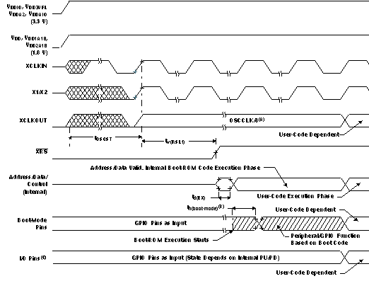
TMS320F28044 td_powres_prs357.gif
Upon power up, SYSCLKOUT is OSCCLK/2. Since the XCLKOUTDIV bits in the XCLK register come up with a reset state of 0, SYSCLKOUT is further divided by 4 before it appears at XCLKOUT. This explains why XCLKOUT = OSCCLK/8 during this phase.
After reset, the boot ROM code samples Boot Mode pins. Based on the status of the Boot Mode pin, the boot code branches to destination memory or boot code function. If boot ROM code executes after power-on conditions (in debugger environment), the boot code execution time is based on the current SYSCLKOUT speed. The SYSCLKOUT will be based on user environment and could be with or without PLL enabled.
See Section 5.9.2 for requirements to ensure a high-impedance state for GPIO pins during power-up.
Figure 5-2 Power-on Reset