ZHCSR22A June 2021 – September 2022 LP876242-Q1
PRODUCTION DATA
- 1 特性
- 2 应用
- 3 说明
- 4 Revision History
- 5 Pin Configuration and Functions
-
6 Specifications
- 6.1 Absolute Maximum Ratings
- 6.2 ESD Ratings
- 6.3 Recommended Operating Conditions
- 6.4 Thermal Information
- 6.5 Internal Low Drop-Out Regulators (LDOVINT)
- 6.6 BUCK1, BUCK2, BUCK3, and BUCK4 Regulators
- 6.7 Reference Generator (REFOUT)
- 6.8 Monitoring Functions
- 6.9 Clocks, Oscillators, and DPLL
- 6.10 Thermal Monitoring and Shutdown
- 6.11 System Control Thresholds
- 6.12 Current Consumption
- 6.13 Digital Input Signal Parameters
- 6.14 Digital Output Signal Parameters
- 6.15 I/O Pullup and Pulldown Resistance
- 6.16 I2C Interface
- 6.17 Serial Peripheral Interface (SPI)
- 25
- 6.18 Typical Characteristics
-
7 Detailed Description
- 7.1 Overview
- 7.2 Functional Block Diagram
- 7.3
Feature Description
- 7.3.1 Input Voltage Monitor
- 7.3.2 Power Resources
- 7.3.3 Residual Voltage Checking
- 7.3.4 Output Voltage Monitor and PGOOD Generation
- 7.3.5 General-Purpose I/Os (GPIO Pins)
- 7.3.6 Thermal Monitoring
- 7.3.7 Interrupts
- 7.3.8
Watchdog (WD)
- 7.3.8.1 Watchdog Fail Counter and Status
- 7.3.8.2 Watchdog Start-Up and Configuration
- 7.3.8.3 MCU to Watchdog Synchronization
- 7.3.8.4 Watchdog Disable Function
- 7.3.8.5 Watchdog Sequence
- 7.3.8.6 Watchdog Trigger Mode
- 7.3.8.7 WatchDog Flow Chart and Timing Diagrams in Trigger Mode
- 55
- 7.3.8.8 Watchdog Question-Answer Mode
- 7.3.9 Error Signal Monitor (ESM)
- 7.4
Device Functional Modes
- 7.4.1
Device State Machine
- 7.4.1.1 Fixed Device Power FSM
- 7.4.1.2
Pre-Configurable Mission States
- 7.4.1.2.1
PFSM Commands
- 7.4.1.2.1.1 REG_WRITE_IMM Command
- 7.4.1.2.1.2 REG_WRITE_MASK_IMM Command
- 7.4.1.2.1.3 REG_WRITE_MASK_PAGE0_IMM Command
- 7.4.1.2.1.4 REG_WRITE_BIT_PAGE0_IMM Command
- 7.4.1.2.1.5 REG_WRITE_WIN_PAGE0_IMM Command
- 7.4.1.2.1.6 REG_WRITE_VOUT_IMM Command
- 7.4.1.2.1.7 REG_WRITE_VCTRL_IMM Command
- 7.4.1.2.1.8 REG_WRITE_MASK_SREG Command
- 7.4.1.2.1.9 SREG_READ_REG Command
- 7.4.1.2.1.10 SREG_WRITE_IMM Command
- 7.4.1.2.1.11 WAIT Command
- 7.4.1.2.1.12 DELAY_IMM Command
- 7.4.1.2.1.13 DELAY_SREG Command
- 7.4.1.2.1.14 TRIG_SET Command
- 7.4.1.2.1.15 TRIG_MASK Command
- 7.4.1.2.1.16 END Command
- 7.4.1.2.2 Configuration Memory Organization and Sequence Execution
- 7.4.1.2.3 Mission State Configuration
- 7.4.1.2.4 Pre-Configured Hardware Transitions
- 7.4.1.2.1
PFSM Commands
- 7.4.1.3 Error Handling Operations
- 7.4.1.4 Device Start-up Timing
- 7.4.1.5 Power Sequences
- 7.4.1.6 First Supply Detection
- 7.4.2 Multi-PMIC Synchronization
- 7.4.1
Device State Machine
- 7.5 Control Interfaces
- 7.6 NVM Configurable Registers
- 7.7 Register Map
- 8 Application and Implementation
- 9 Device and Documentation Support
- 10Mechanical, Packaging, and Orderable Information
7.5.3 Serial Peripheral Interface (SPI)
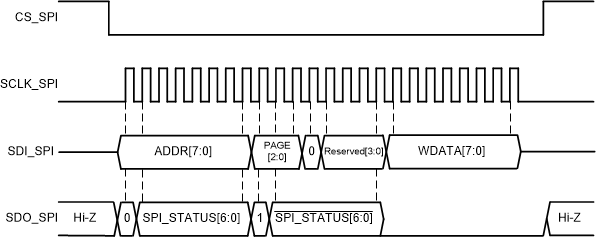
The device supports SPI serial-bus interface and it operates as a peripheral device. The MCU in the system acts as the controller device. A single read and write transmission consists of 24-bit write and read cycles (32-bit if CRC is enabled) in the following order:
- Bits 1-8: ADDR[7:0], Register address
- Bits 9-11: PAGE[2:0], Page address for register
- Bit 12: Read/Write definition, 0 = WRITE, 1 = READ.
- Bits 13-16: RESERVED[4:0], Reserved, use all zeros.
- For Write: Bits 17-24: WDATA[7:0], write data
- For Write with CRC enabled: Bits 25-32: R_CRC[7:0], CRC error code calculated from bits 1-24 sent by the controller device (i.e. the MCU). See Section 7.5.1.
- For Read: Bits 17-24: RDATA[7:0], read data
- For Read with CRC enabled: Bits 25-32: T_CRC[7:0], CRC error code calculated from bits 1-16 sent by the controller device (i.e. the MCU), and bits 17-24, sent by the peripheral device (i.e. the LP876242-Q1). See Section 7.5.1.
In parallel with ADDR[7:0], PAGE[2:0], Read/Write definition and RESERVED[3:0] bits the device sends 16-bit interrupt status using SDO_SPI pin in the following order:
- Bit 1: always 0
- Bits 2-8: status of several interrupts and EN_DRV pin
- Bit 9: always 1
- Bits 10-16: status of several interrupts and EN_DRV pin, with opposite polarity
The status signals are in INT_SPI_STATUS register:
- Bit 8: always 0
- Bit 7: COMM_ADR_ERR_SWINT
- Bit 6: COMM_CRC_ERR_SWINT
- Bit 5: COMM_FRM_ERR_SWINT
- Bit 4: ESM_MCU_PIN_SWINT
- Bit 3: TWARN_SWINT
- Bit 2: WD_SWINT
- Bit 1: EN_DRV_STAT
EN_DRV_STAT bit is showing the live state of the EN_DRV pin, whereas all other status bits are latched in the same way as interrupts indicated with nINT pin. The latched status bits in INT_SPI_STATUS register are cleared by writing 1 to the latched bit. Bits 10-16 are sent for redundancy for bits 2-8 with opposite polarity. Bits 10-16 are always correlating with bits 2-8 and do not change during communication even when the status signal changes.
The embedded CRC filed can be enabled or disabled from the protocol by setting the I2C1_SPI_CRC_EN register bit to '1' - enabled, '0' - disabled. The default of this bit is configurable through the NVM.
The SDO_SPI output is in a high-impedance state when the CS_SPI pin is high. When the CS_SPI pin is low, the SDO_SPI output is always driven low except when the RDATA or SCRC bits are sent. When the RDATA or SCRC bits are sent, the SDO_SPI output is driven accordingly.
The address, page, data, and CRC are transmitted MSB first. The chip-select signal (CS_SPI) must be low during the cycle transmission. The CS_SPI signal resets the interface when it is high, and must be taken high between successive cycles. Data is clocked in on the rising edge of the SCK_SPI clock signal and it is clocked out on the falling edge of SCK_SPI clock signal.
The SPI Timing diagram shows the timing information for these signals.
 Figure 7-56 SPI
Write Cycle
 Figure 7-58 SPI
Read Cycle