ZHCSRC3B December 2022 – March 2025 IWRL6432
PRODUCTION DATA
- 1
- 1 特性
- 2 应用
- 3 说明
- 4 功能方框图
- 5 器件比较
- 6 终端配置和功能
-
7 规格
- 7.1 绝对最大额定值
- 7.2 ESD 等级
- 7.3 上电小时数 (POH)
- 7.4 建议运行条件
- 7.5 一次性可编程 (OTP) 电子保险丝的 VPP 规格
- 7.6 电源规格
- 7.7 节电模式
- 7.8 每个电压轨的峰值电流要求
- 7.9 射频规格
- 7.10 支持的 DFE 特性
- 7.11 CPU 规格
- 7.12 热阻特性
- 7.13 时序和开关特性
- 8 详细说明
- 9 监控和诊断
- 10应用、实施和布局
- 11器件和文档支持
- 12修订历史记录
- 13机械、封装和可订购信息
7.13.3.1 时钟规格
需要外部时钟源(即 CLKP 需要一个 40MHz 晶体或外部振荡器)来进行初始启动并作为器件中托管的内部 APLL 的参考。连接到器件引脚的外部晶体图 7-10 显示了晶体的实现情况。
 图 7-10 晶体实现方式
注:
应该选择图 7-10 中的负载电容器 Cf1 和 Cf2,以满足方程式 1 的要求。公式中的 CL 是晶体制造商指定的负载。用于实现振荡器电路的所有分立式元件应尽可能靠近关联的振荡器 CLKP 和 CLKM 引脚放置。
方程式 1. 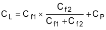
表 7-17 列出了时钟晶体的电气特性。
表 7-17 晶体电气特性(振荡器模式)
| 名称 | 说明 | 最小值 | 典型值 | 最大值 | 单位 |
|---|---|---|---|---|---|
| fP | 并联谐振晶体频率 | 40 | MHz | ||
| CL | 晶体负载电容 | 5 | 8 | 12 | pF |
| ESR | 晶体 ESR | 50 | Ω | ||
| 温度范围 | 预期工作温度范围 | -40 | 105 | °C | |
| 频率容差 | 晶体频率容差(1)(2)(3) | -200 | 200 | ppm | |
| 驱动电平 | 50 | 200 | µW | ||
(1) 晶体制造商的规格必须满足此要求。
(2) 包括晶体的初始容差、温漂、老化以及由于负载电容不正确而导致的频率牵引。
(3) 晶体容差会影响雷达传感器精度。
如果将外部时钟用作时钟资源,则信号仅馈送到 CLKP 引脚;CLKM 接地。当 40MHz 时钟由外部馈送时,相位噪声要求非常重要。表 7-18列出了外部时钟信号的电气特性。
表 7-18 外部时钟模式规格
| 参数 | 规格 | 单位 | |||
|---|---|---|---|---|---|
| 最小值 | 典型值 | 最大值 | |||
| 输入时钟: 外部交流耦合正弦波或直流耦合方波相位噪声,以 40MHz 为基准 |
频率 | 40 | MHz | ||
| 交流振幅 | 700 | 1200 | mV (pp) | ||
| DCVil | 0.00 | 0.20 | V | ||
| DCVih | 1.6 | 1.95 | V | ||
| 1kHz 时的相位噪声 | -132 | dBc/Hz | |||
| 10kHz 时的相位噪声 | -143 | dBc/Hz | |||
| 100kHz 时的相位噪声 | -152 | dBc/Hz | |||
| 1MHz 时的相位噪声 | -153 | dBc/Hz | |||
| 占空比 | 35 | 65 | % | ||
| 频率容差 | -200 | 200 | ppm | ||