SLUSFR7 August 2025 BQ24810
PRODUCTION DATA
- 1
- 1 Features
- 2 Applications
- 3 Description
- 4 Pin Configuration and Functions
- 5 Specifications
-
6 Detailed Description
- 6.1 Overview
- 6.2 Functional Block Diagram
- 6.3
Feature Description
- 6.3.1 Device Power Up
- 6.3.2 System Power Selection
- 6.3.3 Current and Power Monitor
- 6.3.4 Processor Hot Indication for CPU Throttling
- 6.3.5 Input Current Dynamic Power Management
- 6.3.6 Two-Level Adapter Current Limit (Peak Power Mode)
- 6.3.7 EMI Switching Frequency Adjust
- 6.3.8 Device Protections Features
- 6.4 Device Functional Modes
- 6.5 Programming
- 6.6
Register Maps
- 6.6.1 Battery-Charger Commands
- 6.6.2 Setting Charger Options
- 6.6.3 ChargeOption1 Register
- 6.6.4 ChargeOption2 Register
- 6.6.5 ChargeOption3 Register
- 6.6.6 ChargeOption4 Register
- 6.6.7 ProchotOption0 Register
- 6.6.8 ProchotOption1 Register
- 6.6.9 ProchotStatus Register
- 6.6.10 Charge Current Register
- 6.6.11 Charge Voltage Register
- 6.6.12 Discharge Current Register
- 6.6.13 Minimum System Voltage Register
- 6.6.14 Input Current Register
- 6.6.15 Register Exceptions
-
7 Application and Implementation
- 7.1 Application Information
- 7.2
Typical Applications
- 7.2.1
Typical System Schematic
- 7.2.1.1 Design Requirements
- 7.2.1.2
Detailed Design Procedure
- 7.2.1.2.1 Adapter Current Sense Filter
- 7.2.1.2.2 Negative Output Voltage Protection
- 7.2.1.2.3 Reverse Input Voltage Protection
- 7.2.1.2.4 Reduce Battery Quiescent Current
- 7.2.1.2.5 CIN Capacitance
- 7.2.1.2.6 L1 Inductor Selection
- 7.2.1.2.7 CBATT Capacitance
- 7.2.1.2.8 Buck Charging Internal Compensation
- 7.2.1.2.9 CSYS Capacitance
- 7.2.1.2.10 Battery Only Boost Internal Compensation
- 7.2.1.2.11 Power MOSFETs Selection
- 7.2.1.2.12 Input Filter Design
- 7.2.1.3 Application Curves
- 7.2.2 Migration from Previous Devices (Does Not Support Battery Only Boost)
- 7.2.1
Typical System Schematic
- 7.3 Power Supply Recommendations
- 7.4 Layout
- 8 Device and Documentation Support
- 9 Revision History
- 10Mechanical, Packaging, and Orderable Information
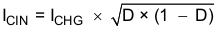
7.2.1.2.5 CIN Capacitance
CIN provides input capacitance when the converter is operating in forward buck charging mode. This should have enough ripple current rating to absorb input switching ripple current. The worst case RMS ripple current is half of the charging current when duty cycle is 0.5. If the converter does not operate at 50% duty cycle, then the worst case capacitor RMS current occurs where the duty cycle is closest to 50% and can be estimated by Equation 6:
Low ESR ceramic capacitor such as X7R or X5R is preferred for input decoupling capacitor and should be placed as close as possible to the drain of the high side switching MOSFET (HIFET). The voltage rating of the capacitor must be higher than normal input voltage level. 25-V rating or higher capacitor is preferred for 19- V to 20-V input voltage. 10- to 20-μF capacitance is suggested for typical of 3- to 4-A charging current.
Ceramic capacitors show a dc-bias effect. This effect reduces the effective capacitance when a dc-bias voltage is applied across a ceramic capacitor, as on the input capacitor of a charger. The effect may lead to a significant capacitance drop, especially for high input voltages and small capacitor packages. See the manufacturer's data sheet about the performance with a dc bias voltage applied. It may be necessary to choose a higher voltage rating or nominal capacitance value in order to get the required value at the operating point.