SLUSFR7 August 2025 BQ24810
PRODUCTION DATA
- 1
- 1 Features
- 2 Applications
- 3 Description
- 4 Pin Configuration and Functions
- 5 Specifications
-
6 Detailed Description
- 6.1 Overview
- 6.2 Functional Block Diagram
- 6.3
Feature Description
- 6.3.1 Device Power Up
- 6.3.2 System Power Selection
- 6.3.3 Current and Power Monitor
- 6.3.4 Processor Hot Indication for CPU Throttling
- 6.3.5 Input Current Dynamic Power Management
- 6.3.6 Two-Level Adapter Current Limit (Peak Power Mode)
- 6.3.7 EMI Switching Frequency Adjust
- 6.3.8 Device Protections Features
- 6.4 Device Functional Modes
- 6.5 Programming
- 6.6
Register Maps
- 6.6.1 Battery-Charger Commands
- 6.6.2 Setting Charger Options
- 6.6.3 ChargeOption1 Register
- 6.6.4 ChargeOption2 Register
- 6.6.5 ChargeOption3 Register
- 6.6.6 ChargeOption4 Register
- 6.6.7 ProchotOption0 Register
- 6.6.8 ProchotOption1 Register
- 6.6.9 ProchotStatus Register
- 6.6.10 Charge Current Register
- 6.6.11 Charge Voltage Register
- 6.6.12 Discharge Current Register
- 6.6.13 Minimum System Voltage Register
- 6.6.14 Input Current Register
- 6.6.15 Register Exceptions
-
7 Application and Implementation
- 7.1 Application Information
- 7.2
Typical Applications
- 7.2.1
Typical System Schematic
- 7.2.1.1 Design Requirements
- 7.2.1.2
Detailed Design Procedure
- 7.2.1.2.1 Adapter Current Sense Filter
- 7.2.1.2.2 Negative Output Voltage Protection
- 7.2.1.2.3 Reverse Input Voltage Protection
- 7.2.1.2.4 Reduce Battery Quiescent Current
- 7.2.1.2.5 CIN Capacitance
- 7.2.1.2.6 L1 Inductor Selection
- 7.2.1.2.7 CBATT Capacitance
- 7.2.1.2.8 Buck Charging Internal Compensation
- 7.2.1.2.9 CSYS Capacitance
- 7.2.1.2.10 Battery Only Boost Internal Compensation
- 7.2.1.2.11 Power MOSFETs Selection
- 7.2.1.2.12 Input Filter Design
- 7.2.1.3 Application Curves
- 7.2.2 Migration from Previous Devices (Does Not Support Battery Only Boost)
- 7.2.1
Typical System Schematic
- 7.3 Power Supply Recommendations
- 7.4 Layout
- 8 Device and Documentation Support
- 9 Revision History
- 10Mechanical, Packaging, and Orderable Information
7.2.1.2.11 Power MOSFETs Selection
Two external N-channel MOSFETs are used for a synchronous switching battery charger. The gate drivers are internally integrated into the IC with 6V of gate drive voltage. 30 V or higher voltage rating MOSFETs are preferred for 19- to 20-V input voltage.
Figure-of-merit (FOM) is usually used for selecting proper MOSFET based on a tradeoff between the conduction loss and switching loss. For the top side MOSFET, FOM is defined as the product of a MOSFET's on-resistance, RDS(ON), and the gate-to-drain charge, QGD. For the bottom side MOSFET, FOM is defined as the product of the MOSFET's on-resistance, RDS(ON), and the total gate charge, QG.
The lower the FOM value, the lower the total power loss. Usually lower RDS(ON) has higher cost with the same package size.
The top-side MOSFET loss includes conduction loss and switching loss. It is a function of duty cycle (D=VOUT/VIN), charging current (ICHG), MOSFET's on-resistance (RDS(ON)), input voltage (VIN), switching frequency (fS), turn on time (ton) and turn off time (toff):

The first item represents the conduction loss. Usually MOSFET RDS(ON) increases by 50% with 100°C junction temperature rise. The second term represents the switching loss. The MOSFET turn-on and turn-off times are given by:

where Qsw is the switching charge, Ion is the turn-on gate driving current and Ioff is the turn-off gate driving current. If the switching charge is not given in MOSFET datasheet, it can be estimated by gate-to-drain charge (QGD) and gate-to-source charge (QGS):

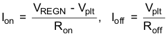
Gate driving current can be estimated by REGN voltage (VREGN), MOSFET plateau voltage (Vplt), total turn-on gate resistance (Ron) and turn-off gate resistance (Roff) of the gate driver:
The conduction loss of the bottom-side MOSFET is calculated with the following equation when it operates in synchronous continuous conduction mode:
When charger operates in non-synchronous mode, the bottom-side MOSFET is off. As a result all the freewheeling current goes through the body-diode of the bottom-side MOSFET. The body diode power loss depends on its forward voltage drop (VF), non-synchronous mode charging current (INONSYNC), and duty cycle (D).
The maximum charging current in non-synchronous mode can be up to 0.25 A for a 10-mΩ charging current sensing resistor or 0.5 A if battery voltage is below 2.5 V. The minimum duty cycle happens at lowest battery voltage. Choose the bottom-side MOSFET with either an internal Schottky or body diode capable of carrying the maximum non-synchronous mode charging current.