ZHCS990C June 2012 – September 2021 TPS54719
PRODUCTION DATA
- 1 特性
- 2 应用
- 3 说明
- 4 Revision History
- 5 Pin Configuration and Functions
- 6 Specifications
-
7 Detailed Description
- 7.1 Overview
- 7.2 Functional Block Diagram
- 7.3
Feature Description
- 7.3.1 Fixed Frequency PWM Control
- 7.3.2 Slope Compensation And Output Current
- 7.3.3 Bootstrap Voltage (Boot) And Low Dropout Operation
- 7.3.4 Error Amplifier
- 7.3.5 Voltage Reference
- 7.3.6 Adjusting The Output Voltage
- 7.3.7 Enable and Adjusting Undervoltage Lockout
- 7.3.8 Slow Start/Tracking Pin
- 7.3.9 Sequencing
- 7.4
Device Functional Modes
- 7.4.1 Constant Switching Frequency And Timing Resistor (RT Pin)
- 7.4.2 Overcurrent Protection
- 7.4.3 Frequency Shift
- 7.4.4 Reverse Overcurrent Protection
- 7.4.5 Power Good (PWRGD Pin)
- 7.4.6 Overvoltage Transient Protection
- 7.4.7 Thermal Shutdown
- 7.4.8 Small Signal Model For Loop Response
- 7.4.9 Simple Small Signal Model For Peak Current Mode Control
- 7.4.10 Small Signal Model For Frequency Compensation
-
8 Application and Implementation
- 8.1 Application Information
- 8.2
Typical Application
- 8.2.1 High Frequency, 1.8-V Output Power Supply Design With Adjusted UVLO
- 8.2.2 Design Requirements
- 8.2.3
Detailed Design Procedure
- 8.2.3.1 Selecting The Switching Frequency
- 8.2.3.2 Output Inductor Selection
- 8.2.3.3 Output Capacitor
- 8.2.3.4 Input Capacitor
- 8.2.3.5 Slow-Start Capacitor
- 8.2.3.6 Bootstrap Capacitor Selection
- 8.2.3.7 Undervoltage Lockout Set Point
- 8.2.3.8 Output Voltage And Feedback Resistors Selection
- 8.2.3.9 Compensation
- 8.2.4 Application Curves
- 9 Power Supply Recommendations
- 10Layout
- 11Device and Documentation Support
- 12Mechanical, Packaging, and Orderable Information
8.2.3.3 Output Capacitor
There are three primary considerations for selecting the value of the output capacitor. The output capacitor determines the modulator pole, the output voltage ripple, and how the regulator responds to a large change in load current. The output capacitance needs to be selected based on the more stringent of these three criteria.
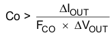
The desired response to a large change in the load current is the first criteria. The output capacitor needs to supply the load with current when the regulator can not. This situation would occur if there are desired hold-up times for the regulator where the output capacitor must hold the output voltage above a certain level for a specified amount of time after the input power is removed. The regulator is temporarily not able to supply sufficient output current if there is a large, fast increase in the current needs of the load, such as transitioning from no load to a full load. The regulator response to the load step change is limited by the control loop bandwidth, FCO. The output capacitor must be sized to supply the extra current without excessive output voltage drop until the control loop can respond to the load change. Equation 25 shows the minimum output capacitance necessary for an instantaneous load step change. Practical circuits will have a slew rate limited load step and will typically require less capacitance.
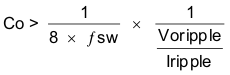
For this example, the transient load response is specified as a 6% change in Vout for a load step from 1.75 A (25%) to 5.25 A (75%), and ΔVout = 0.06 × 1.8 = 108 mV. For a load step slew rate of 30 mA / µsec, 2 × 22 µF is sufficient to meet the voltage drop requirement. The ESR of the output capacitor is ignored as the ESR of ceramic capacitors is small.
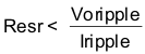
Equation 26 calculates the minimum output capacitance needed to meet the output voltage ripple specification. In this case, the maximum output voltage ripple is 30 mV. Under this requirement, Equation 26 yields 14 µF.
where:
- ΔIout is the change in output current
- Fsw is the regulators switching frequency
- ΔVout is the allowable change in the output voltage
- Vripple is the maximum allowable output voltage ripple
- Iripple is the inductor ripple current
Equation 27 calculates the maximum ESR an output capacitor can have to meet the output voltage ripple specification. Equation 27 indicates the ESR should be less than 28.6 mΩ. In this case, the ESR of the ceramic capacitor is much less than 17.9 mΩ.
Additional capacitance de-ratings for aging, temperature and DC bias should be factored in which increases this minimum value. For this example, two 22-μF 10-V X5R ceramic capacitors with 3 mΩ of ESR are used.
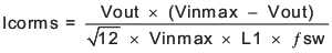
Capacitors generally have limits to the amount of ripple current they can handle without failing or producing excess heat. An output capacitor that can support the inductor ripple current must be specified. Some capacitor data sheets specify the RMS (Root Mean Square) value of the maximum ripple current. Equation 28 can be used to calculate the RMS ripple current the output capacitor needs to support. For this application, Equation 28 yields 485 mA.