ZHCS990C June 2012 – September 2021 TPS54719
PRODUCTION DATA
- 1 特性
- 2 应用
- 3 说明
- 4 Revision History
- 5 Pin Configuration and Functions
- 6 Specifications
-
7 Detailed Description
- 7.1 Overview
- 7.2 Functional Block Diagram
- 7.3
Feature Description
- 7.3.1 Fixed Frequency PWM Control
- 7.3.2 Slope Compensation And Output Current
- 7.3.3 Bootstrap Voltage (Boot) And Low Dropout Operation
- 7.3.4 Error Amplifier
- 7.3.5 Voltage Reference
- 7.3.6 Adjusting The Output Voltage
- 7.3.7 Enable and Adjusting Undervoltage Lockout
- 7.3.8 Slow Start/Tracking Pin
- 7.3.9 Sequencing
- 7.4
Device Functional Modes
- 7.4.1 Constant Switching Frequency And Timing Resistor (RT Pin)
- 7.4.2 Overcurrent Protection
- 7.4.3 Frequency Shift
- 7.4.4 Reverse Overcurrent Protection
- 7.4.5 Power Good (PWRGD Pin)
- 7.4.6 Overvoltage Transient Protection
- 7.4.7 Thermal Shutdown
- 7.4.8 Small Signal Model For Loop Response
- 7.4.9 Simple Small Signal Model For Peak Current Mode Control
- 7.4.10 Small Signal Model For Frequency Compensation
-
8 Application and Implementation
- 8.1 Application Information
- 8.2
Typical Application
- 8.2.1 High Frequency, 1.8-V Output Power Supply Design With Adjusted UVLO
- 8.2.2 Design Requirements
- 8.2.3
Detailed Design Procedure
- 8.2.3.1 Selecting The Switching Frequency
- 8.2.3.2 Output Inductor Selection
- 8.2.3.3 Output Capacitor
- 8.2.3.4 Input Capacitor
- 8.2.3.5 Slow-Start Capacitor
- 8.2.3.6 Bootstrap Capacitor Selection
- 8.2.3.7 Undervoltage Lockout Set Point
- 8.2.3.8 Output Voltage And Feedback Resistors Selection
- 8.2.3.9 Compensation
- 8.2.4 Application Curves
- 9 Power Supply Recommendations
- 10Layout
- 11Device and Documentation Support
- 12Mechanical, Packaging, and Orderable Information
7.4.10 Small Signal Model For Frequency Compensation
The TPS54719 uses a transconductance amplifier for the error amplifier and readily supports two of the commonly used frequency compensation circuits. The compensation circuits are shown in Figure 7-11. The Type 2 circuits are most likely implemented in high bandwidth power supply designs using low-ESR output capacitors. In Type 2A, one additional high frequency pole is added to attenuate high frequency noise.
 Figure 7-11 Types Of Frequency Compensation
The design guidelines for TPS54719 loop compensation are as follows:
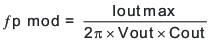
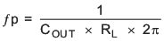
- The modulator pole, fpmod, and the esr zero, fz1,
must be calculated using Equation 14 and Equation 15. Derating the output capacitor (COUT) can be needed if the output
voltage is a high percentage of the capacitor rating. Use the capacitor
manufacturer information to derate the capacitor value. Use Equation 16 and Equation 17 to estimate a starting point for the crossover frequency, fc. Equation 16 is the geometric mean of the modulator pole and the esr zero and Equation 17 is the mean of modulator pole and the switching frequency. Use the lower
value of Equation 16 or Equation 17 as the maximum crossover frequency. Equation 14.
 Equation 15.
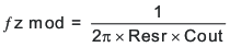 Equation 16.
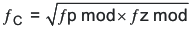 Equation 17.
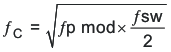
- R3 can be determined by Equation 18.
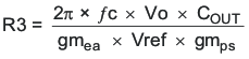
where:
- gmea is the amplifier gain (250 μA/V)
- gmps is the power stage gain (25 A/V)
- Place a compensation zero at the dominant pole
 . C1 can be determined by
Equation 19.
. C1 can be determined by
Equation 19.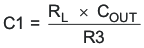
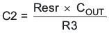
- C2 is optional. It can be used to cancel the zero
from the ESR of Co. Equation 20.