ZHCS990C June 2012 – September 2021 TPS54719
PRODUCTION DATA
- 1 特性
- 2 应用
- 3 说明
- 4 Revision History
- 5 Pin Configuration and Functions
- 6 Specifications
-
7 Detailed Description
- 7.1 Overview
- 7.2 Functional Block Diagram
- 7.3
Feature Description
- 7.3.1 Fixed Frequency PWM Control
- 7.3.2 Slope Compensation And Output Current
- 7.3.3 Bootstrap Voltage (Boot) And Low Dropout Operation
- 7.3.4 Error Amplifier
- 7.3.5 Voltage Reference
- 7.3.6 Adjusting The Output Voltage
- 7.3.7 Enable and Adjusting Undervoltage Lockout
- 7.3.8 Slow Start/Tracking Pin
- 7.3.9 Sequencing
- 7.4
Device Functional Modes
- 7.4.1 Constant Switching Frequency And Timing Resistor (RT Pin)
- 7.4.2 Overcurrent Protection
- 7.4.3 Frequency Shift
- 7.4.4 Reverse Overcurrent Protection
- 7.4.5 Power Good (PWRGD Pin)
- 7.4.6 Overvoltage Transient Protection
- 7.4.7 Thermal Shutdown
- 7.4.8 Small Signal Model For Loop Response
- 7.4.9 Simple Small Signal Model For Peak Current Mode Control
- 7.4.10 Small Signal Model For Frequency Compensation
-
8 Application and Implementation
- 8.1 Application Information
- 8.2
Typical Application
- 8.2.1 High Frequency, 1.8-V Output Power Supply Design With Adjusted UVLO
- 8.2.2 Design Requirements
- 8.2.3
Detailed Design Procedure
- 8.2.3.1 Selecting The Switching Frequency
- 8.2.3.2 Output Inductor Selection
- 8.2.3.3 Output Capacitor
- 8.2.3.4 Input Capacitor
- 8.2.3.5 Slow-Start Capacitor
- 8.2.3.6 Bootstrap Capacitor Selection
- 8.2.3.7 Undervoltage Lockout Set Point
- 8.2.3.8 Output Voltage And Feedback Resistors Selection
- 8.2.3.9 Compensation
- 8.2.4 Application Curves
- 9 Power Supply Recommendations
- 10Layout
- 11Device and Documentation Support
- 12Mechanical, Packaging, and Orderable Information
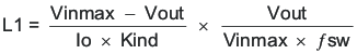
8.2.3.2 Output Inductor Selection
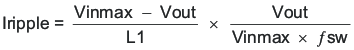
The inductor selected works for the entire TPS54719 input voltage range. To calculate the value of the output inductor, use Equation 21. KIND is a coefficient that represents the amount of inductor ripple current relative to the maximum output current. The inductor ripple current is filtered by the output capacitor. Therefore, choosing high inductor ripple currents impacts the selection of the output capacitor since the output capacitor must have a ripple current rating equal to or greater than the inductor ripple current. In general, the inductor ripple value is at the discretion of the designer; however, KIND is normally from 0.1 to 0.3 for the majority of applications.
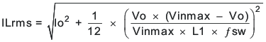
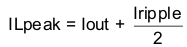
For this design example, use KIND = 0.3 and the minimum inductor value is calculated to be 1.2 μH. For this design, a larger standard value of 1.5 μH was chosen. For the output filter inductor, it is important that the RMS current and saturation current ratings not be exceeded. The RMS and peak inductor current can be found from Equation 23 and Equation 24.
For this design, the RMS inductor current is 7.017 A and the peak inductor current is 7.84 A. The chosen inductor is a Würth 744311150 1.5 µH. It has a saturation current rating of 14 A (30% inductance loss) and an RMS current rating of 11 A ( 40 °C temperature rise). The series resistance is 6.6 mΩ typical.
The current flowing through the inductor is the inductor ripple current plus the output current. During power up, faults, or transient load conditions, the inductor current can increase above the calculated peak inductor current level calculated above. In transient conditions, the inductor current can increase up to the switch current limit of the device. For this reason, the most conservative approach is to specify an inductor with a saturation current rating equal to or greater than the switch current limit rather than the peak inductor current.