ZHCS990C June 2012 – September 2021 TPS54719
PRODUCTION DATA
- 1 特性
- 2 应用
- 3 说明
- 4 Revision History
- 5 Pin Configuration and Functions
- 6 Specifications
-
7 Detailed Description
- 7.1 Overview
- 7.2 Functional Block Diagram
- 7.3
Feature Description
- 7.3.1 Fixed Frequency PWM Control
- 7.3.2 Slope Compensation And Output Current
- 7.3.3 Bootstrap Voltage (Boot) And Low Dropout Operation
- 7.3.4 Error Amplifier
- 7.3.5 Voltage Reference
- 7.3.6 Adjusting The Output Voltage
- 7.3.7 Enable and Adjusting Undervoltage Lockout
- 7.3.8 Slow Start/Tracking Pin
- 7.3.9 Sequencing
- 7.4
Device Functional Modes
- 7.4.1 Constant Switching Frequency And Timing Resistor (RT Pin)
- 7.4.2 Overcurrent Protection
- 7.4.3 Frequency Shift
- 7.4.4 Reverse Overcurrent Protection
- 7.4.5 Power Good (PWRGD Pin)
- 7.4.6 Overvoltage Transient Protection
- 7.4.7 Thermal Shutdown
- 7.4.8 Small Signal Model For Loop Response
- 7.4.9 Simple Small Signal Model For Peak Current Mode Control
- 7.4.10 Small Signal Model For Frequency Compensation
-
8 Application and Implementation
- 8.1 Application Information
- 8.2
Typical Application
- 8.2.1 High Frequency, 1.8-V Output Power Supply Design With Adjusted UVLO
- 8.2.2 Design Requirements
- 8.2.3
Detailed Design Procedure
- 8.2.3.1 Selecting The Switching Frequency
- 8.2.3.2 Output Inductor Selection
- 8.2.3.3 Output Capacitor
- 8.2.3.4 Input Capacitor
- 8.2.3.5 Slow-Start Capacitor
- 8.2.3.6 Bootstrap Capacitor Selection
- 8.2.3.7 Undervoltage Lockout Set Point
- 8.2.3.8 Output Voltage And Feedback Resistors Selection
- 8.2.3.9 Compensation
- 8.2.4 Application Curves
- 9 Power Supply Recommendations
- 10Layout
- 11Device and Documentation Support
- 12Mechanical, Packaging, and Orderable Information
8.2.3.4 Input Capacitor
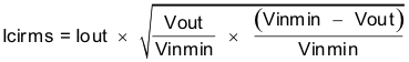
The TPS54719 requires a high quality ceramic, type X5R or X7R, input decoupling capacitor of at least 10 μF of effective capacitance and in some applications a bulk capacitance. The effective capacitance includes any DC bias effects. The voltage rating of the input capacitor must be greater than the maximum input voltage. The capacitor must also have a ripple current rating greater than the maximum input current ripple of the TPS54719. The input ripple current can be calculated using Equation 29.
The value of a ceramic capacitor varies significantly over temperature and the amount of DC bias applied to the capacitor. The capacitance variations due to temperature can be minimized by selecting a dielectric material that is stable over temperature. X5R and X7R ceramic dielectrics are usually selected for power regulator capacitors because they have a high capacitance to volume ratio and are fairly stable over temperature. The output capacitor must also be selected with the DC bias taken into account. The capacitance value of a capacitor decreases as the DC bias across a capacitor increases.
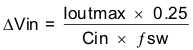
For this example design, ceramic capacitors with at least a 10-V voltage rating are required to support the maximum input voltage. For this example, two 10-μF and one 0.1-μF, 10-V capacitors in parallel have been selected. The input capacitance value determines the input ripple voltage of the regulator. The input voltage ripple can be calculated using Equation 30. Using the design example values, Ioutmax = 7 A, Cin = 20 μF, and Fsw = 500 kHz, yields an input voltage ripple of 174 mV and a rms input ripple current of 3.43 A.