ZHCS990C June 2012 – September 2021 TPS54719
PRODUCTION DATA
- 1 特性
- 2 应用
- 3 说明
- 4 Revision History
- 5 Pin Configuration and Functions
- 6 Specifications
-
7 Detailed Description
- 7.1 Overview
- 7.2 Functional Block Diagram
- 7.3
Feature Description
- 7.3.1 Fixed Frequency PWM Control
- 7.3.2 Slope Compensation And Output Current
- 7.3.3 Bootstrap Voltage (Boot) And Low Dropout Operation
- 7.3.4 Error Amplifier
- 7.3.5 Voltage Reference
- 7.3.6 Adjusting The Output Voltage
- 7.3.7 Enable and Adjusting Undervoltage Lockout
- 7.3.8 Slow Start/Tracking Pin
- 7.3.9 Sequencing
- 7.4
Device Functional Modes
- 7.4.1 Constant Switching Frequency And Timing Resistor (RT Pin)
- 7.4.2 Overcurrent Protection
- 7.4.3 Frequency Shift
- 7.4.4 Reverse Overcurrent Protection
- 7.4.5 Power Good (PWRGD Pin)
- 7.4.6 Overvoltage Transient Protection
- 7.4.7 Thermal Shutdown
- 7.4.8 Small Signal Model For Loop Response
- 7.4.9 Simple Small Signal Model For Peak Current Mode Control
- 7.4.10 Small Signal Model For Frequency Compensation
-
8 Application and Implementation
- 8.1 Application Information
- 8.2
Typical Application
- 8.2.1 High Frequency, 1.8-V Output Power Supply Design With Adjusted UVLO
- 8.2.2 Design Requirements
- 8.2.3
Detailed Design Procedure
- 8.2.3.1 Selecting The Switching Frequency
- 8.2.3.2 Output Inductor Selection
- 8.2.3.3 Output Capacitor
- 8.2.3.4 Input Capacitor
- 8.2.3.5 Slow-Start Capacitor
- 8.2.3.6 Bootstrap Capacitor Selection
- 8.2.3.7 Undervoltage Lockout Set Point
- 8.2.3.8 Output Voltage And Feedback Resistors Selection
- 8.2.3.9 Compensation
- 8.2.4 Application Curves
- 9 Power Supply Recommendations
- 10Layout
- 11Device and Documentation Support
- 12Mechanical, Packaging, and Orderable Information
8.2.3.9 Compensation
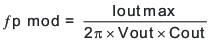
There are several possible methods to design closed loop compensation for dc/dc converters. For the ideal current mode control, the design equations can be easily simplified. The power stage gain is constant at low frequencies, and rolls off at -20 dB/decade above the modulator pole frequency. The power stage phase is 0 degrees at low frequencies and starts to fall one decade below the modulator pole frequency reaching a minimum of -90 degrees one decade above the modulator pole frequency. The modulator pole is a simple pole shown in Equation 34.
For the TPS54719, most circuits will have relatively high amounts of slope compensation. As more slope compensation is applied, the power stage characteristics will deviate from the ideal approximations. The phase loss of the power stage will now approach -180 degrees, making compensation more difficult. The power stage transfer function can be solved but it is a tedious hand calculation that does not lend itself to simple approximations. It is best to use Pspice or TINA-TI to accurately model the power stage gain and phase so that a reliable compensation circuit can be designed. That is the technique used in this design procedure. Using the pspice model of (insert link here). Apply the values calculated previously to the output filter components of L1, C9 and C10. Set Rload to the appropriate value. For this design, L1 = 1.5 µH. C9 and C10 are set to 22 µF each, and the ESR is set to 3 mΩ. The Rload resistor is 1.8 V / 3.5 A = 514 mΩ for one half rated load. Now the power stage characteristic can be plotted as shown in Figure 8-1.
 Figure 8-1 Power Stage Gain And Phase Characteristics
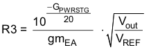
For this design, the intended crossover frequency is 50 kHz. From the power stage gain and phase plots, the gain at 50 kHz is 2.04 dB and the phase is about –135 degrees. For 60 degrees of phase margin, additional phase boost from a feedforward capacitor in parallel with the upper resistor of the voltage set point divider will be required. R3 sets the gain of the compensated error amplifier to be equal and opposite the power stage gain at crossover. The required value of R3 can be calculated from Equation 35.
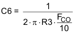
To maximize phase gain, the compensator zero is placed one decade below the crossover frequency of 50 kHz. The required value for C6 is given by Equation 36.
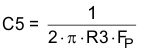
To maximize phase gain the high frequency pole is placed one decade above the crossover frequency of 50 kHz. The pole can also be useful to offset the ESR of aluminum electrolytic output capacitors. The value for C5 can be calculated from Equation 37.
For maximum phase boost, the pole frequency FP will typically be one decade above the intended crossover frequency FCO.
The feedforward capacitor, C11, is used to increase the phase boost at crossover above what is normally available from Type II compensation. It places an additional zero/pole pair located at Equation 38 and Equation 39.
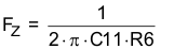
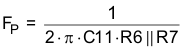
This zero and pole pair is not independent. Once the zero location is chosen, the pole is fixed as well. For optimum performance, the zero and pole should be located symmetrically about the intended crossover frequency. The required value for C10 can calculated from Equation 40.
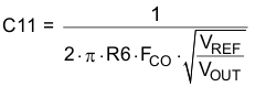
For this design the calculated values for the compensation components are R3 = 5.49 kΩ, C6 = 5600 pF, C5 = 56 pF, and C11 = 270 pF.