SPRABI1D January 2018 – July 2022 66AK2E05 , 66AK2G12 , 66AK2H06 , 66AK2H12 , 66AK2H14 , 66AK2L06 , AM5K2E02 , AM5K2E04 , SM320C6678-HIREL , TMS320C6652 , TMS320C6654 , TMS320C6655 , TMS320C6657 , TMS320C6670 , TMS320C6671 , TMS320C6672 , TMS320C6674 , TMS320C6678
- Trademarks
- 1 Introduction
- 2 Background
- 3 Migrating Designs From DDR2 to DDR3 (Features and Comparisons)
- 4 Prerequisites
- 5 Package Selection
-
6 Physical Design and Implementation
- 6.1 Electrical Connections
- 6.2 Signal Terminations
- 6.3
Mechanical Layout and Routing Considerations
- 6.3.1
Routing Considerations – SDRAMs
- 6.3.1.1 Mechanical Layout – SDRAMs
- 6.3.1.2 Stack Up – SDRAMs
- 6.3.1.3 Routing Rules – General Overview (SDRAMs)
- 6.3.1.4 Routing Rules – Address and Command Lines (SDRAMs)
- 6.3.1.5 Routing Rules – Control Lines (SDRAMs)
- 6.3.1.6 Routing Rules – Data Lines (SDRAMs)
- 6.3.1.7 Routing Rules – Clock Lines (SDRAMs)
- 6.3.1.8 Routing Rules – Power (SDRAMs)
- 6.3.1.9 Write Leveling Limit Impact on Routing – KeyStone I
- 6.3.1.10 Round-Trip Delay Impact on Routing – KeyStone I
- 6.3.1.11 Write Leveling Limit Impact on Routing – KeyStone II
- 6.3.1.12 Round-Trip Delay Impact on Routing – KeyStone II
- 6.3.2
Routing Considerations – UDIMMs
- 6.3.2.1 Mechanical Layout – UDIMMs
- 6.3.2.2 Stack Up – UDIMMs
- 6.3.2.3 Routing Rules – General Overview (UDIMMs)
- 6.3.2.4 Routing Rules – Address and Command Lines (UDIMMs)
- 6.3.2.5 Routing Rules – Control Lines (UDIMMs)
- 6.3.2.6 Routing Rules – Data Lines (UDIMMs)
- 6.3.2.7 Routing Rules – Clock Lines (UDIMMs)
- 6.3.2.8 Routing Rules – Power (UDIMMs)
- 6.3.2.9 Write-Leveling Limit Impact on Routing
- 6.3.1
Routing Considerations – SDRAMs
- 6.4 Timing Considerations
- 6.5 Impedance Considerations
- 6.6 Switching and Output Considerations
- 7 Simulation and Modeling
- 8 Power
- 9 Disclaimers
- 10References
- 11Revision History
4.7.2.1 Overshoot and Undershoot Example Calculations
The following is provided as an example of the necessary steps to calculate the overshoots and undershoots for any waveform.
Assumptions: VDD = 1.5 V; VSS = 0.00 V; Vref = 0.75 V (VDD/2)
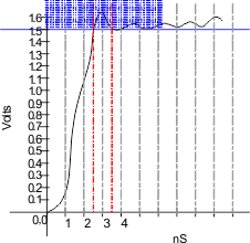
Overshoot example (Figure 4-3)
- Determine amplitude over VDD
- Determine the duration of the amplitude
- Calculate the final value
- OS = Amplitude × Duration
- OS = 180 mV × 1 ns
- OS = 0.18 V-ns
- Compare results to the applicable
SDRAM row and column (Section 4.7.2) paying attention to speed grade and signal type differences. If the SDRAM
speed was DDR3-800 or DDR3-1066 and this were a data, clock, strobe, or mask
net, the overshoot would be acceptable. In the case of data, clock, strobe, or
mask DDR3-1333 and DDR3-1600 speed grades, this level of overshoot is not
acceptable. Note: This level is acceptable for all speed grades of control and address lines.
 Figure 4-3 Signal Overshoot
Calculations
Figure 4-3 Signal Overshoot
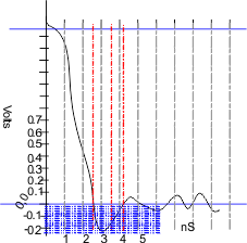
CalculationsUndershoot example (Figure 4-4)
- Determine amplitude under VSS
- Determine the duration of the amplitude
- Calculate the final value
- US = Amplitude × Duration
- US = 215 mV × 1.5 ns
- US = 0.322 V-ns
- Compare results to the applicable
SDRAM row and column (Section 4.7.2 paying attention to speed grade and signal type differences). If the SDRAM
was DDR3-800 or DDR3-1066 and this were a data net, this overshoot would be
acceptable. In the case of DDR3-1333 and DDR3-1600, this level of undershoot is
not acceptable. Compare results to the applicable SDRAM row and column (notice
speed grade differences). This example undershoot is unacceptable for all speed
grades for all data, clock, strobe, and mask signals. It is acceptable for all
speed grades of address and control signals. Note: This level is acceptable for all speed grades of control and address lines.
 Figure 4-4 Signal Undershoot
Calculations