SPRABI1D January 2018 – July 2022 66AK2E05 , 66AK2G12 , 66AK2H06 , 66AK2H12 , 66AK2H14 , 66AK2L06 , AM5K2E02 , AM5K2E04 , SM320C6678-HIREL , TMS320C6652 , TMS320C6654 , TMS320C6655 , TMS320C6657 , TMS320C6670 , TMS320C6671 , TMS320C6672 , TMS320C6674 , TMS320C6678
- Trademarks
- 1 Introduction
- 2 Background
- 3 Migrating Designs From DDR2 to DDR3 (Features and Comparisons)
- 4 Prerequisites
- 5 Package Selection
-
6 Physical Design and Implementation
- 6.1 Electrical Connections
- 6.2 Signal Terminations
- 6.3
Mechanical Layout and Routing Considerations
- 6.3.1
Routing Considerations – SDRAMs
- 6.3.1.1 Mechanical Layout – SDRAMs
- 6.3.1.2 Stack Up – SDRAMs
- 6.3.1.3 Routing Rules – General Overview (SDRAMs)
- 6.3.1.4 Routing Rules – Address and Command Lines (SDRAMs)
- 6.3.1.5 Routing Rules – Control Lines (SDRAMs)
- 6.3.1.6 Routing Rules – Data Lines (SDRAMs)
- 6.3.1.7 Routing Rules – Clock Lines (SDRAMs)
- 6.3.1.8 Routing Rules – Power (SDRAMs)
- 6.3.1.9 Write Leveling Limit Impact on Routing – KeyStone I
- 6.3.1.10 Round-Trip Delay Impact on Routing – KeyStone I
- 6.3.1.11 Write Leveling Limit Impact on Routing – KeyStone II
- 6.3.1.12 Round-Trip Delay Impact on Routing – KeyStone II
- 6.3.2
Routing Considerations – UDIMMs
- 6.3.2.1 Mechanical Layout – UDIMMs
- 6.3.2.2 Stack Up – UDIMMs
- 6.3.2.3 Routing Rules – General Overview (UDIMMs)
- 6.3.2.4 Routing Rules – Address and Command Lines (UDIMMs)
- 6.3.2.5 Routing Rules – Control Lines (UDIMMs)
- 6.3.2.6 Routing Rules – Data Lines (UDIMMs)
- 6.3.2.7 Routing Rules – Clock Lines (UDIMMs)
- 6.3.2.8 Routing Rules – Power (UDIMMs)
- 6.3.2.9 Write-Leveling Limit Impact on Routing
- 6.3.1
Routing Considerations – SDRAMs
- 6.4 Timing Considerations
- 6.5 Impedance Considerations
- 6.6 Switching and Output Considerations
- 7 Simulation and Modeling
- 8 Power
- 9 Disclaimers
- 10References
- 11Revision History
6.3.1.7 Routing Rules – Clock Lines (SDRAMs)
The following rules must be followed when routing clock nets in a DDR3 design:
- CK/ CK pairs must be routed differentially.
- 100-Ω (±5%) differential impedance required on all clock pairs.
- Each CK/ CK pair is managed as a separate routing group.
- Each CK/ CK pair must be routed to all SDRAMs within a single rank.
- All nets in the clock fly-by groups must route along the same path from the controller to each SDRAM sequentially and then to an AC VTT termination.
- All clock pairs must be length-matched from the controller to each SDRAM separately within ±1 mils of each other.
- All nets in the clock fly-by group must have the same number of vias in each length-matched segment.
- Clock pair stubs must be less than 40 mils and length-matched within ±mil.
- All clock pair nets must route adjacent to a solid ground plane.
Table 6-6 shows the numeric routing rules listed above for data lines.
Table 6-6 Clock Lane Numeric Routing Rules
| Rule Number | Parameter | Value | Unit |
|---|---|---|---|
| 1 | Net Impedance (differential) | 100 | Ω |
| 2 | Skew between CK/ CK pairs | ±1 | mils |
| 3 | Stub length | <40 | mils |
| 4 | Stub skew | ±1 |
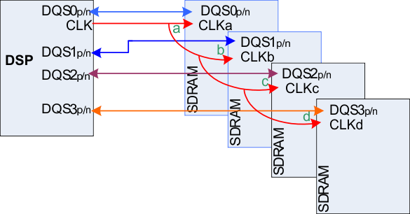
Figure 6-4 shows the required DDRCLKOUT and DQ/ DQS → DQ/DQS/ DQS routing from the DSP to SDRAMs for a single-rank topology.
 Figure 6-4 DDRCLKOUT and DQ/
DQS Routing From the DSP to SDRAMs