SPRAAV1C May 2009 – March 2020 AM3703 , AM3715 , OMAP3503 , OMAP3515 , OMAP3525 , OMAP3530
-
PCB Design Guidelines for 0.4mm Package-On-Package (PoP) Packages, Part I
- Trademarks
- 1 Using This Guide
- 2 A Word of Caution
- 3 A Team Sport
- 4 Be Wary of Quotes
- 5 Don’t Forget Your CAD Tools
- 6 Metric Vs English
- 7 PCB Fab Limits
- 8 Routing and Layer Stackup
- 9 OMAP35x 0.4mm Pitch
- 10 Pad Type
- 11 PCB Pad Dimensions for 0.4mm BGA Package
- 12 Multiple BGA Packages
- 13 Etch Traps and Heat Sinks
- 14 Vias and VIP
- 15 Laser Blind Vias
- 16 Filled Vias
- 17 Know Your Tools
- 18 BeagleBoard
- 19 BeagleBoard Views
- 20 OMAP35x Decoupling
- 21 PCB Finishes for High Density Interconnect (HDI)
- 22 Real World Second Opinion
- 23 Acknowledgments
- 24 References
- Revision History
14 Vias and VIP
One of the greatest benefits from package-on-package technology is the elimination of the complex, expensive, and challenging task of routing high-speed memory lines from under the processor out to memory. Instead, the memory sits on top of the processor and the connections are automatically made during assembly.
Except for the outer perimeter balls, routing for the BeagleBoard is done with VIP technology. Although this was once a feared and expensive technology, recent studies and advances have eliminated nearly all of the problems. In fact, VIP is becoming the dominant technology for high density boards and is providing a cost effective alternative to conventional and offset vias.
The VIP methodology places the via directly under the device’s balls. However, this requires another step to seal the via to prevent blowouts and voids. For the BeagleBoard, non-conductive, epoxy-filled vias were used.
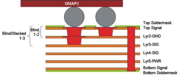
The BeagleBoard uses only through-hole vias from top to bottom, blind vias from top to layer 2, and stacked vias from top layer to layer 3. It does not use buried vias. All vias are laser drilled.
 Figure 13. BeagleBoard Via Example