SPRAAV1C May 2009 – March 2020 AM3703 , AM3715 , OMAP3503 , OMAP3515 , OMAP3525 , OMAP3530
-
PCB Design Guidelines for 0.4mm Package-On-Package (PoP) Packages, Part I
- Trademarks
- 1 Using This Guide
- 2 A Word of Caution
- 3 A Team Sport
- 4 Be Wary of Quotes
- 5 Don’t Forget Your CAD Tools
- 6 Metric Vs English
- 7 PCB Fab Limits
- 8 Routing and Layer Stackup
- 9 OMAP35x 0.4mm Pitch
- 10 Pad Type
- 11 PCB Pad Dimensions for 0.4mm BGA Package
- 12 Multiple BGA Packages
- 13 Etch Traps and Heat Sinks
- 14 Vias and VIP
- 15 Laser Blind Vias
- 16 Filled Vias
- 17 Know Your Tools
- 18 BeagleBoard
- 19 BeagleBoard Views
- 20 OMAP35x Decoupling
- 21 PCB Finishes for High Density Interconnect (HDI)
- 22 Real World Second Opinion
- 23 Acknowledgments
- 24 References
- Revision History
18 BeagleBoard
The BeagleBoard is an open-source hardware platform based on the Texas Instruments' OMAP35x. The platform is a complete single board computer suitable for software development and debug. Use the following link for additional information, including the hardware schematics and Gerber files: http://beagleboard.org. Also consider subscribing to the BeagleBoard RSS feed.
 Figure 16. BeagleBoard.org
 The BeagleBoard is used to illustrate the use of the 0.4 mm PCB design guidelines and the assembly guidelines discussed in PCB Assembly Guidelines for 0.4mm Package-On-Package (PoP) Packages, Part II.
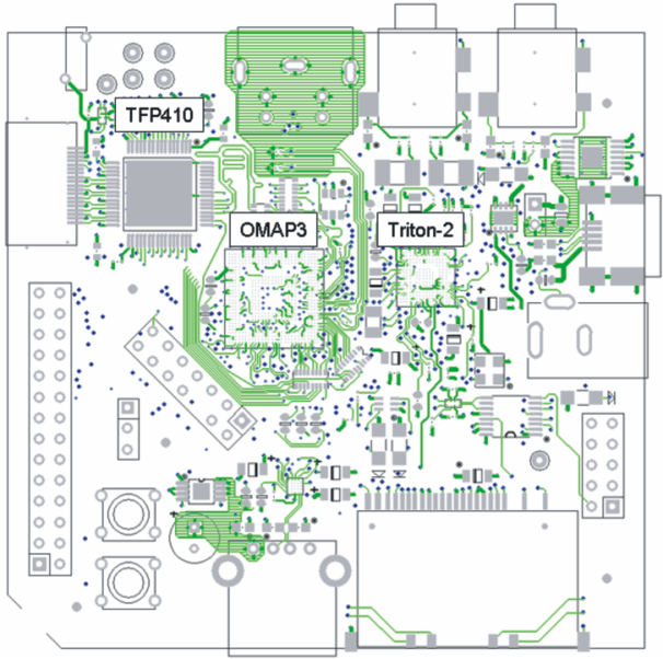
Figure 17 shows the board layout. Subsequent sections discuss each layer as it is used to route the BeagleBoard with special attention given to the area under the OMAP35x device. The overall board dimensions are 3 inches by 3.1 inches and it is a 6 layer board.
Copies of the Gerber files and schematics from the BeagleBoard website provide an example of a real layout that has gone to production.
 Figure 17. Top Layer BeagleBoard Layout