SPRAAV1C May 2009 – March 2020 AM3703 , AM3715 , OMAP3503 , OMAP3515 , OMAP3525 , OMAP3530
-
PCB Design Guidelines for 0.4mm Package-On-Package (PoP) Packages, Part I
- Trademarks
- 1 Using This Guide
- 2 A Word of Caution
- 3 A Team Sport
- 4 Be Wary of Quotes
- 5 Don’t Forget Your CAD Tools
- 6 Metric Vs English
- 7 PCB Fab Limits
- 8 Routing and Layer Stackup
- 9 OMAP35x 0.4mm Pitch
- 10 Pad Type
- 11 PCB Pad Dimensions for 0.4mm BGA Package
- 12 Multiple BGA Packages
- 13 Etch Traps and Heat Sinks
- 14 Vias and VIP
- 15 Laser Blind Vias
- 16 Filled Vias
- 17 Know Your Tools
- 18 BeagleBoard
- 19 BeagleBoard Views
- 20 OMAP35x Decoupling
- 21 PCB Finishes for High Density Interconnect (HDI)
- 22 Real World Second Opinion
- 23 Acknowledgments
- 24 References
- Revision History
12 Multiple BGA Packages
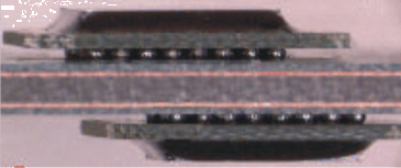
When BGA packages are placed on the top and bottom layers, do not place one BGA package directly underneath another BGA package. The temperature cycle board level reliability degrades if overlap of package footprint occurs.
 Figure 9. Multiple BGA Pacbages on PCB Should Be Off-Set
 Several studies, including the one referenced here, show that temperature cycle board-level-reliability (BLR) performance degrades if there is an overlap of package footprints. A small BGA opposite a large BGA or QFP, with its footprint within the unpopulated I/O shadow of the larger package, has temperature cycle performance similar to that of a single-side board assembly.
 Figure 10. Multiple BGA Packages on PCB Should not Be Overlapped
 For additional information on this concept, see section 5.4, Single-Sided Soldering and Double-Sided Soldering, of NEC’s, Semicondutor Device Mount Manual, http://www.necel.com/pkg/en/mount/ (this link is no longer good).