ZHCSI67D May 2018 – December 2019 MSP430FR2153 , MSP430FR2155 , MSP430FR2353 , MSP430FR2355
PRODUCTION DATA.
- 1器件概述
- 2Device Comparison
- 3Terminal Configuration and Functions
-
4Specifications
- 4.1 Absolute Maximum Ratings
- 4.2 ESD Ratings
- 4.3 Recommended Operating Conditions
- 4.4 Active Mode Supply Current Into VCC Excluding External Current
- 4.5 Active Mode Supply Current Per MHz
- 4.6 Low-Power Mode LPM0 Supply Currents Into VCC Excluding External Current
- 4.7 Low-Power Mode LPM3 and LPM4 Supply Currents (Into VCC) Excluding External Current
- 4.8 Low-Power Mode LPMx.5 Supply Currents (Into VCC) Excluding External Current
- 4.9 Production Distribution of LPM Supply Currents
- 4.10 Typical Characteristics - Current Consumption Per Module
- 4.11 Thermal Resistance Characteristics
- 4.12
Timing and Switching Characteristics
- 4.12.1 Power Supply Sequencing
- 4.12.2 Reset Timing
- 4.12.3 Clock Specifications
- 4.12.4 Internal Shared Reference
- 4.12.5 General-Purpose I/Os
- 4.12.6 Digital I/O Typical Characteristics
- 4.12.7 Timer_B
- 4.12.8
eUSCI
- Table 4-14 eUSCI (UART Mode) Clock Frequencies
- Table 4-15 eUSCI (UART Mode) Switching Characteristics
- Table 4-16 eUSCI (SPI Master Mode) Clock Frequency
- Table 4-17 eUSCI (SPI Master Mode) Switching Characteristics
- Table 4-18 eUSCI (SPI Slave Mode) Switching Characteristics
- Table 4-19 eUSCI (I2C Mode) Switching Characteristics
- 4.12.9 ADC
- 4.12.10 Enhanced Comparator (eCOMP)
- 4.12.11 Smart Analog Combo (SAC) (MSP430FR235x Devices Only)
- 4.12.12 FRAM
- 4.12.13 Emulation and Debug
-
5Detailed Description
- 5.1 CPU
- 5.2 Operating Modes
- 5.3 Interrupt Vector Addresses
- 5.4 Memory Organization
- 5.5 Bootloader (BSL)
- 5.6 JTAG Standard Interface
- 5.7 Spy-Bi-Wire Interface (SBW)
- 5.8 FRAM
- 5.9 Memory Protection
- 5.10
Peripherals
- 5.10.1 Power Management Module (PMM) and On-Chip Reference Voltages
- 5.10.2 Clock System (CS) and Clock Distribution
- 5.10.3 General-Purpose Input/Output Port (I/O)
- 5.10.4 Watchdog Timer (WDT)
- 5.10.5 System Module (SYS)
- 5.10.6 Cyclic Redundancy Check (CRC)
- 5.10.7 Interrupt Compare Controller (ICC)
- 5.10.8 Enhanced Universal Serial Communication Interface (eUSCI_A0, eUSCI_A1, eUSCI_B0, eUSCI_B1)
- 5.10.9 Timers (Timer0_B3, Timer1_B3, Timer2_B3, Timer3_B7)
- 5.10.10 Backup Memory (BKMEM)
- 5.10.11 Real-Time Clock (RTC) Counter
- 5.10.12 12-Bit Analog-to-Digital Converter (ADC)
- 5.10.13 Enhanced Comparator
- 5.10.14 Manchester Function Module (MFM)
- 5.10.15 Smart Analog Combo (SAC) (MSP430FR235x Devices Only)
- 5.10.16 eCOMP0, eCOMP1, SAC0, SAC1, SAC2, and SAC3 Interconnection (MSP430FR235x Devices Only)
- 5.10.17 Cross-Chip Interconnection (SACx are MSP430FR235x Devices Only)
- 5.10.18 Embedded Emulation Module (EEM)
- 5.10.19 Peripheral File Map
- 5.11 Input/Output Diagrams
- 5.12 Device Descriptors (TLV)
- 5.13 Identification
- 6Applications, Implementation, and Layout
- 7器件和文档支持
- 8机械、封装和可订购信息
封装选项
机械数据 (封装 | 引脚)
散热焊盘机械数据 (封装 | 引脚)
订购信息
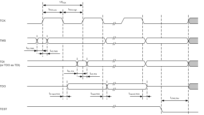
Table 4-29 JTAG, 4-Wire Interface
over recommended ranges of supply voltage and operating free-air temperature (unless otherwise noted) (see Figure 4-18)| PARAMETER | DEVICE GRADE | VCC | MIN | TYP | MAX | UNIT | |
|---|---|---|---|---|---|---|---|
| fTCK | TCK input frequency (1) | I, T | 2.0 V, 3.0 V | 0 | 10 | MHz | |
| tTCK,Low | Spy-Bi-Wire low clock pulse duration | I, T | 2.0 V, 3.0 V | 15 | ns | ||
| tTCK,high | Spy-Bi-Wire high clock pulse duration | I, T | 2.0 V, 3.0 V | 15 | ns | ||
| tSU,TMS | TMS setup time (before rising edge of TCK) | I, T | 2.0 V, 3.0 V | 11 | ns | ||
| tHD,TMS | TMS hold time (after rising edge of TCK) | I, T | 2.0 V, 3.0 V | 3 | ns | ||
| tSU,TDI | TDI setup time (before rising edge of TCK) | I, T | 2.0 V, 3.0 V | 13 | ns | ||
| tHD,TDI | TDI hold time (after rising edge of TCK) | I, T | 2.0 V, 3.0 V | 5 | ns | ||
| tz-Valid,TDO | TDO high impedance to valid output time (after falling edge of TCK) | I, T | 2.0 V, 3.0 V | 26 | ns | ||
| tValid,TDO | TDO to new valid output time (after falling edge of TCK) | I, T | 2.0 V, 3.0 V | 26 | ns | ||
| tValid-Z,TDO | TDO valid to high impedance output time (after falling edge of TCK) | I, T | 2.0 V, 3.0 V | 26 | ns | ||
| tJTAG,Ret | Spy-Bi-Wire return to normal operation time | I, T | 2.0 V, 3.0 V | 15 | 100 | µs | |
| Rinternal | Internal pulldown resistance on TEST | I, T | 2.0 V, 3.0 V | 20 | 35 | 50 | kΩ |
 Figure 4-18 JTAG 4-Wire Timing