ZHCSIH0C December   2017  – June 2021 LP87702-Q1

PRODUCTION DATA  

  1. 特性
  2. 应用
  3. 说明
  4. Revision History
  5. 说明(续)
  6. Pin Configuration and Functions
  7. Specifications
    1. 7.1 Absolute Maximum Ratings
    2. 7.2 ESD Ratings
    3. 7.3 Recommended Operating Conditions
    4. 7.4 Thermal Information
    5. 7.5 Electrical Characteristics
    6. 7.6 I2C Serial Bus Timing Parameters
    7. 7.7 Typical Characteristics
  8. Detailed Description
    1. 8.1 Overview
    2. 8.2 Functional Block Diagram
    3. 8.3 Feature Descriptions
      1. 8.3.1  Step-Down DC/DC Converters
        1. 8.3.1.1 Overview
        2. 8.3.1.2 Transition Between PWM and PFM Modes
        3. 8.3.1.3 Buck Converter Load Current Measurement
      2. 8.3.2  Boost Converter
      3. 8.3.3  Spread-Spectrum Mode
      4. 8.3.4  Sync Clock Functionality
      5. 8.3.5  Power-Up
      6. 8.3.6  Buck and Boost Control
        1. 8.3.6.1 Enabling and Disabling Converters
        2. 8.3.6.2 Changing Buck Output Voltage
      7. 8.3.7  Enable and Disable Sequences
      8. 8.3.8  Window Watchdog
      9. 8.3.9  Device Reset Scenarios
      10. 8.3.10 Diagnostics and Protection Features
        1. 8.3.10.1 Voltage Monitorings
        2. 8.3.10.2 Interrupts
        3. 8.3.10.3 Power-Good Information to Interrupt, PG0, and PG1 Pins
          1. 8.3.10.3.1 PGx Pin Gated (Unusual) Mode
          2. 8.3.10.3.2 PGx Pin Operation in Continuous Mode
          3. 8.3.10.3.3 Summary of PG0, PG1 Gated, and Continuous Operating Modes
        4. 8.3.10.4 Warning Interrupts for System Level Diagnostics
          1. 8.3.10.4.1 Output Power Limit
          2. 8.3.10.4.2 Thermal Warning
        5. 8.3.10.5 Protections Causing Converter Disable
          1. 8.3.10.5.1 Short-Circuit and Overload Protection
          2. 8.3.10.5.2 Overvoltage Protection
          3. 8.3.10.5.3 Thermal Shutdown
        6. 8.3.10.6 Protections Causing Device Power Down
          1. 8.3.10.6.1 Undervoltage Lockout
      11. 8.3.11 OTP Error Correction
      12. 8.3.12 Operation of GPO Signals
      13. 8.3.13 Digital Signal Filtering
    4. 8.4 Device Functional Modes
      1. 8.4.1 Modes of Operation
    5. 8.5 Programming
      1. 8.5.1 I2C-Compatible Interface
        1. 8.5.1.1 Data Validity
        2. 8.5.1.2 Start and Stop Conditions
        3. 8.5.1.3 Transferring Data
        4. 8.5.1.4 I2C-Compatible Chip Address
        5. 8.5.1.5 Auto Increment Feature
    6. 8.6 Register Maps
      1. 8.6.1 Register Descriptions
        1. 8.6.1.1 LP8770_map Registers
  9. Application and Implementation
    1. 9.1 Application Information
    2. 9.2 Typical Application
      1. 9.2.1 Design Requirements
      2. 9.2.2 Detailed Design Procedure
        1. 9.2.2.1 Application Components
          1. 9.2.2.1.1 Inductor Selection
          2. 9.2.2.1.2 Buck Input Capacitor Selection
          3. 9.2.2.1.3 Buck Output Capacitor Selection
          4. 9.2.2.1.4 Boost Input Capacitor Selection
          5. 9.2.2.1.5 Boost Output Capacitor Selection
          6. 9.2.2.1.6 Supply Filtering Components
      3. 9.2.3 Current Limit vs Maximum Output Current
      4. 9.2.4 Application Curves
  10. 10Power Supply Recommendations
  11. 11Layout
    1. 11.1 Layout Guidelines
    2. 11.2 Layout Example
  12. 12Device and Documentation Support
    1. 12.1 第三方产品免责声明
    2. 12.2 Receiving Notification of Documentation Updates
    3. 12.3 支持资源
    4. 12.4 Trademarks
    5. 12.5 Electrostatic Discharge Caution
    6. 12.6 Glossary
  13. 13Mechanical, Packaging, and Orderable Information

封装选项

机械数据 (封装 | 引脚)
散热焊盘机械数据 (封装 | 引脚)
订购信息

Application Curves

Unless otherwise specified: VIN = 3.3 V, VOUT_BUCK = 1 V, VOUT_BOOST = 5 V, TA = 25°C, ƒSW-setting 4 MHz, L0 = L1 = 0.47 µH (TOKO DFE252012PD-R47M), L2 = 1 µH (TFM252012ALMA1R0), COUT_BUCK, CPOL_BUCK, and COUT_BOOST = 22 µF. Measurements are done using connections in Figure 9-1.
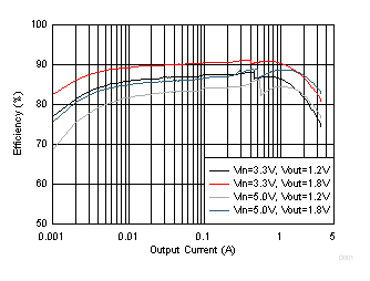
Unless otherwise specified: VIN = 3.3 V, VOUT_BUCK = 1 V, VOUT_BOOST = 5 V, TA = 25°C, ƒSW-setting 4 MHz, L0 = L1 = 0.47 µH (TOKO DFE252012PD-R47M), L2 = 1 µH (TFM252012ALMA1R0), COUT_BUCK, CPOL_BUCK, and COUT_BOOST = 22 µF. Measurements are done using connections in Figure 9-1.GUID-1AF75F3E-5492-493A-8E80-3EADDEB63373-low.gif
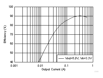
Figure 9-3 Buck Efficiency in AUTO (PFM/PWM) Mode. Unless otherwise specified: VIN = 3.3 V, VOUT_BUCK = 1 V, VOUT_BOOST = 5 V, TA = 25°C, ƒSW-setting 4 MHz, L0 = L1 = 0.47 µH (TOKO DFE252012PD-R47M), L2 = 1 µH (TFM252012ALMA1R0), COUT_BUCK, CPOL_BUCK, and COUT_BOOST = 22 µF. Measurements are done using connections in Figure 9-1.
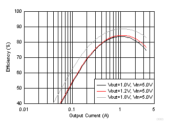
GUID-097E34B7-F250-45FE-93CE-ACCEE46F3D13-low.gif
VIN = 5 V
Figure 9-5 Buck Efficiency in Forced PWM Mode
GUID-126660DC-2366-430E-91F3-AD759A7E9B4D-low.gif
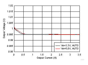
VOUT = 1 V
Figure 9-7 Buck Output Voltage vs Load Current in AUTO Mode
GUID-B14D4F67-C8DA-41C8-9F77-80B7FA15E171-low.gif
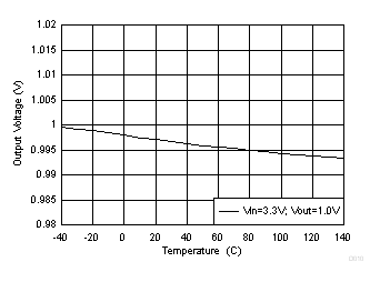
Figure 9-9 Buck Output Voltage vs Temperature
GUID-A884FC35-5C87-466F-B409-461AB0BE04B5-low.png
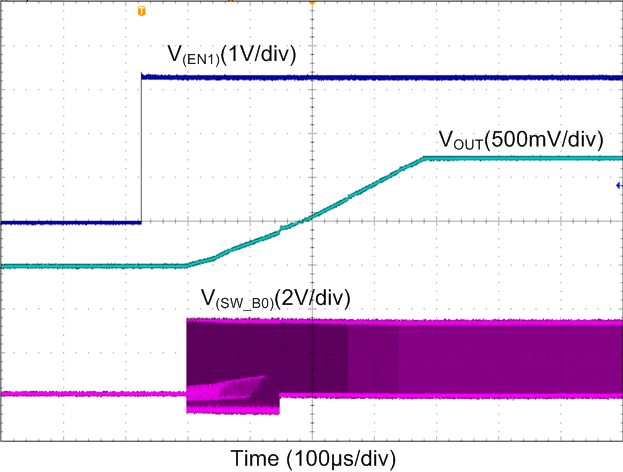
RLOAD = 1 Ω
Figure 9-11 Buck Start-up with EN1, Forced-PWM
GUID-B63E2BB2-1188-455C-9F1D-183A961F066C-low.png
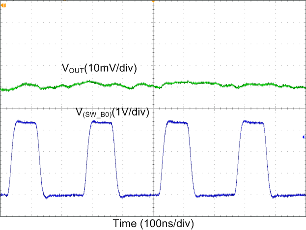
VOUT = 1.2 VIOUT = 500 mA
Figure 9-13 Buck Output Voltage Ripple, Forced-PWM Mode
GUID-3E6D23F5-ED92-4824-A8F2-7783F7FEC707-low.png
VOUT = 1.2 V
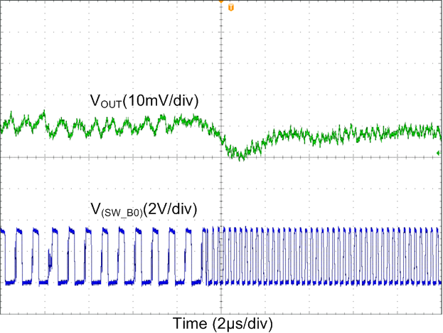
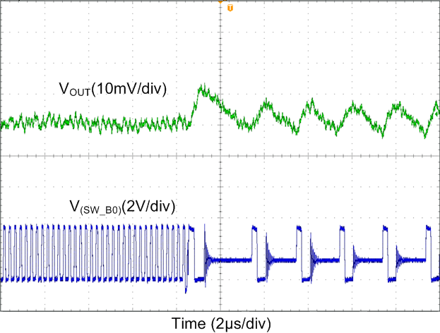
Figure 9-15 Buck Transient from PFM-to-PWM Mode
GUID-7F6448C6-A577-4C2D-A040-954C7C26E0FA-low.png
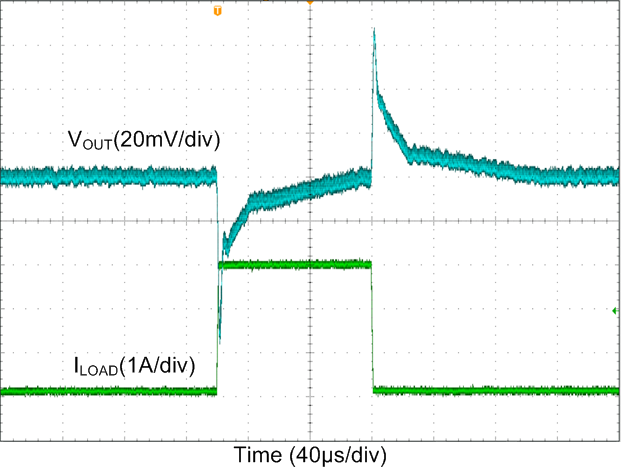
IOUT = 0 A → 3 A → 0 ATR = TF = 1 µsVOUT = 1 V
Figure 9-17 Buck Transient Load Step Response, Forced-PWM Mode
GUID-286D839E-BDCC-4250-8423-DB36A4136278-low.png
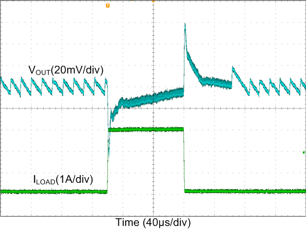
IOUT = 0 A → 3 A → 0 ATR = TF = 1 µsVOUT = 1 V
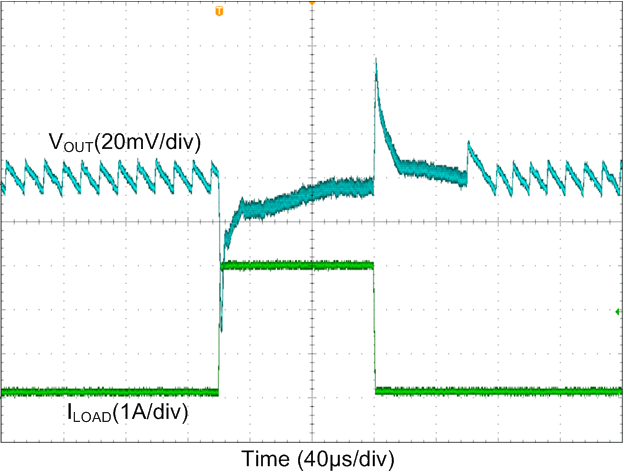
Figure 9-19 Buck Transient Load Step Response, Auto Mode
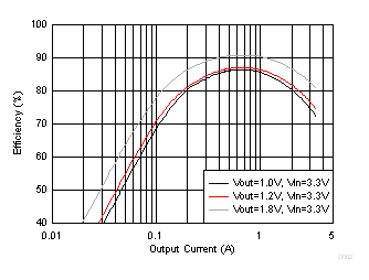
GUID-DB16CB47-7BE4-42EE-8B23-4F6B8E15D9D6-low.gif
Figure 9-21 Boost Efficiency
GUID-36A96F7C-74AB-467D-ABE2-51E43637B782-low.gif
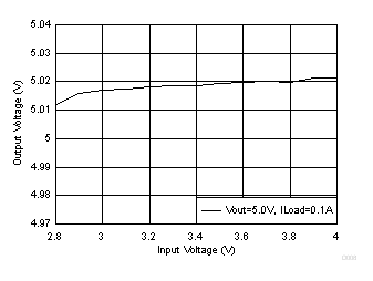
IOUT = 0.1 A
Figure 9-23 Boost Output Voltage vs Input Voltage
GUID-FA7745E8-AC89-44B7-8116-C3BDBC236213-low.png
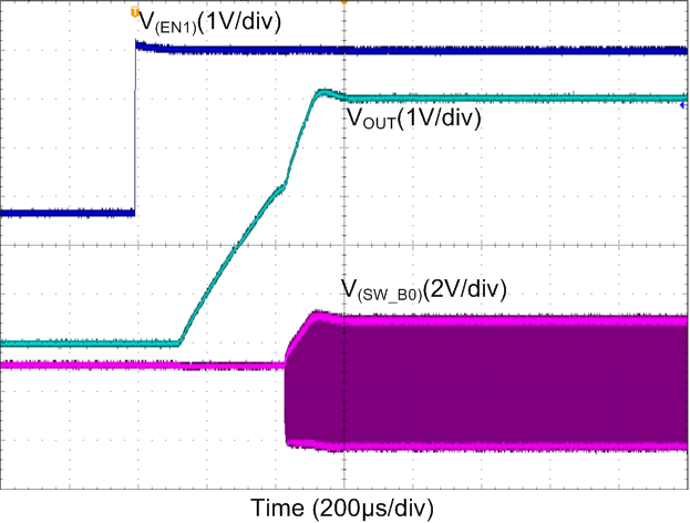
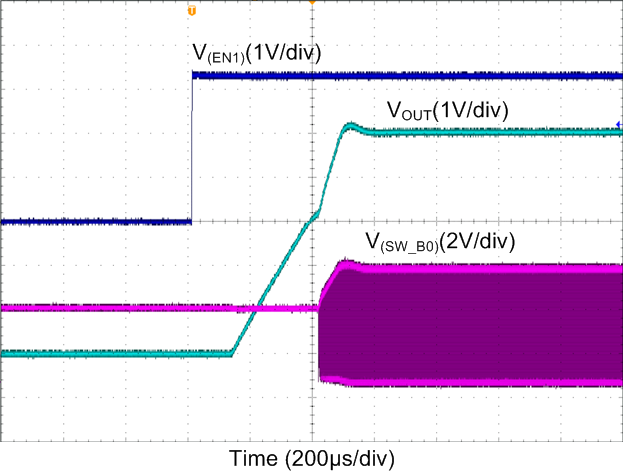
RLOAD = 50 Ω
Figure 9-25 Boost Start-up With EN1, Forced-PWM
GUID-168338FA-261F-476A-AF3E-AAFEB52BF07A-low.png
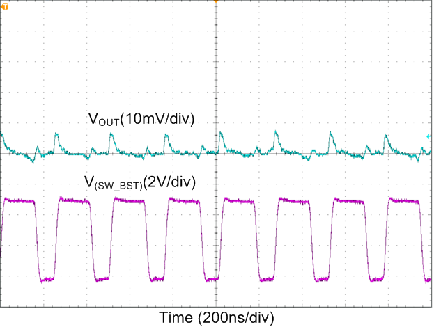
IOUT = 0.1 A
Figure 9-27 Boost Output Voltage Ripple
GUID-6F72C947-04EA-4292-8F8A-12B188A1EED8-low.gif
VIN = 3.3 V
Figure 9-4 Buck Efficiency in Forced PWM Mode
GUID-697F7800-DE17-4617-8E98-A6621AFA5A5B-low.gif
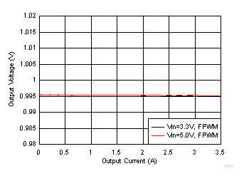
VOUT = 1 V
Figure 9-6 Buck Output Voltage vs Load Current in Forced PWM Mode
GUID-BBF8384D-3D69-49D0-9A5C-E6950828CC4A-low.gif
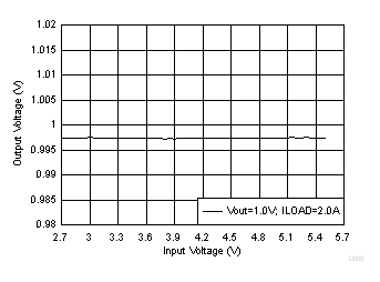
Figure 9-8 Buck Output Voltage vs Input Voltage in PWM Mode
GUID-7DA6300F-4B9D-4E4C-8CFD-FA9621A04F23-low.png
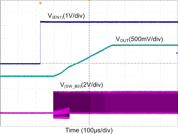
IOUT = 0 A
Figure 9-10 Buck Start-up with EN1, Forced-PWM
GUID-A014E1B3-C5A2-4178-8EAF-E0EBAFCC8877-low.png
RLOAD = 1 Ω
Figure 9-12 Buck Shutdown with EN1, Forced-PWM
GUID-EC1441DD-FFA2-4966-B4A8-E9BEA3F2A1D0-low.png
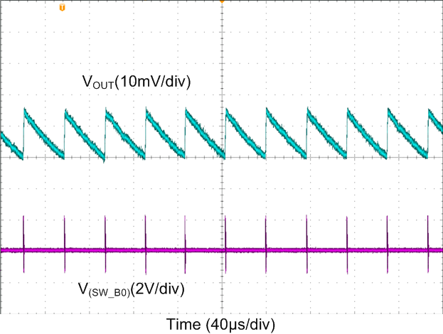
VOUT = 1.2 VIOUT = 10 mA
Figure 9-14 Buck Output Voltage Ripple, PFM Mode
GUID-84823F04-C027-4BF9-BA8B-5711FAE3CB34-low.png
VOUT = 1.2 V
Figure 9-16 Buck Transient from PWM-to-PFM Mode
GUID-8F68C201-9365-4081-8AFC-AE13EB3655B5-low.png
IOUT = 0 A → 3 A → 0 ATR = TF = 1 µsVOUT = 1.2 V
Figure 9-18 Buck Transient Load Step Response, Forced-PWM Mode
GUID-790726E6-FF03-460F-950F-616B2B57FE59-low.png
VOUT = 1.2 V
Figure 9-20 Buck Transient Load Step Response, Auto Mode
GUID-F257CA5E-8B29-4DAE-A4D8-6B781B107F22-low.gif
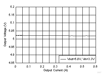
Figure 9-22 Boost Output Voltage vs Load Current
GUID-BC78BA3C-9613-4C14-992E-FC894AFB51BA-low.png
IOUT = 0 A
Figure 9-24 Boost Start-up With EN1, Forced-PWM
GUID-E5CD01F2-511D-4650-9744-33352D26C245-low.png
RLOAD = 50 Ω
Figure 9-26 Boost Shutdown With EN1, Forced-PWM
GUID-E69F249F-574B-4F20-ADF7-FB35F6A241DD-low.png
IOUT = 0 A → 0.25 A → 0 ATR = TF = 1 µs
Figure 9-28 Boost Transient Load Step Response