ZHCSIH0C December 2017 – June 2021 LP87702-Q1
PRODUCTION DATA
- 1 特性
- 2 应用
- 3 说明
- 4 Revision History
- 5 说明(续)
- 6 Pin Configuration and Functions
- 7 Specifications
-
8 Detailed Description
- 8.1 Overview
- 8.2 Functional Block Diagram
- 8.3
Feature Descriptions
- 8.3.1 Step-Down DC/DC Converters
- 8.3.2 Boost Converter
- 8.3.3 Spread-Spectrum Mode
- 8.3.4 Sync Clock Functionality
- 8.3.5 Power-Up
- 8.3.6 Buck and Boost Control
- 8.3.7 Enable and Disable Sequences
- 8.3.8 Window Watchdog
- 8.3.9 Device Reset Scenarios
- 8.3.10 Diagnostics and Protection Features
- 8.3.11 OTP Error Correction
- 8.3.12 Operation of GPO Signals
- 8.3.13 Digital Signal Filtering
- 8.4 Device Functional Modes
- 8.5 Programming
- 8.6 Register Maps
- 9 Application and Implementation
- 10Power Supply Recommendations
- 11Layout
- 12Device and Documentation Support
- 13Mechanical, Packaging, and Orderable Information
8.3.1.1 Overview
The LP87702-Q1 includes two high-efficiency step-down DC/DC converters. The buck converters deliver 0.7-V to 3.36-V regulated voltage rails from 2.8-V to 5.5-V input-supply voltage. The converters are designed for flexibility; most of the functions are programmable, thus optimizing the converter operation for each application:
- DVS support with programmable slew rate
- Automatic mode control based on the loading (PWM or PFM mode)
- Forced PWM mode option
- Optional external clock input to minimize crosstalk
- Optional spread spectrum technique to reduce EMI
- Synchronous rectification
- Current mode loop with PI compensator
- Soft start
- Programmable output voltage monitoring with maskable interrupt and selectable connection PG0 or PG1
- Average output current sensing (for PFM entry and load current measurement)
Some of the key parameters that can be programmed through the registers (with default values set by OTP bits):
- Output voltage
- Forced PWM operation
- Switch current limit
- Output voltage slew rate
- Enable and disable delays with ENx pin control
There are two modes of operation for the buck converters, depending on the output current required: pulse width modulation (PWM) and pulse-frequency modulation (PFM). The converter operates in PWM mode at high load currents of approximately 520 mA or higher. Lighter output current loads will cause the converter to automatically switch into PFM mode for reduced current consumption when forced PWM mode is disabled. The forced PWM mode can be selected to maintain fixed switching frequency at all load currents. When buck is disabled, buck output is isolated from the input voltage rail. Output has an optional pulldown resistor.
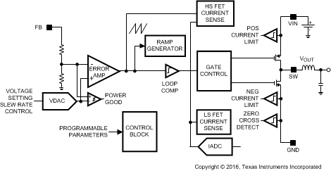
Figure 8-1 shows a block diagram of a single buck converter.
 Figure 8-1 Detailed Block Diagram Showing One Buck Converter