ZHCSPC5 October 2022 LM51231-Q1
PRODUCTION DATA
- 1 特性
- 2 应用
- 3 说明
- 4 Revision History
- 5 Pin Configuration and Functions
- 6 Specifications
-
7 Detailed Description
- 7.1 Overview
- 7.2 Functional Block Diagram
- 7.3
Feature Description
- 7.3.1 Device Enable/Disable (EN, VH Pin)
- 7.3.2 High Voltage VCC Regulator (BIAS, VCC Pin)
- 7.3.3 Light Load Switching Mode Selection (MODE Pin)
- 7.3.4 VOUT Range Selection (RANGE Pin)
- 7.3.5 Line Undervoltage Lockout (UVLO Pin)
- 7.3.6 Fast Restart using VCC HOLD (VH Pin)
- 7.3.7 Adjustable Output Regulation Target (VOUT, TRK, VREF Pin)
- 7.3.8 Overvoltage Protection (VOUT Pin)
- 7.3.9 Power Good Indicator (PGOOD Pin)
- 7.3.10 Dynamically Programmable Switching Frequency (RT)
- 7.3.11 External Clock Synchronization (SYNC Pin)
- 7.3.12 Programmable Spread Spectrum (DITHER Pin)
- 7.3.13 Programmable Soft-start (SS Pin)
- 7.3.14 Wide Bandwidth Transconductance Error Amplifier and PWM (TRK, COMP Pin)
- 7.3.15 Current Sensing and Slope Compensation (CSP, CSN Pin)
- 7.3.16 Constant Peak Current Limit (CSP, CSN Pin)
- 7.3.17 Maximum Duty Cycle and Minimum Controllable On-time Limits
- 7.3.18 MOSFET Drivers, Integrated Boot Diode, and Hiccup Mode Fault Protection (LO, HO, HB Pin)
- 7.3.19 Thermal Shutdown Protection
- 7.4 Device Functional Modes
- 8 Application and Implementation
- 9 Device and Documentation Support
- 10Mechanical, Packaging, and Orderable Information
7.3.12 Programmable Spread Spectrum (DITHER Pin)
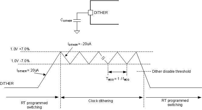
The device provides an optional programmable spread spectrum (clock dithering) function that is activated by connecting a capacitor between DITHER and AGND. A triangular waveform centered at 1.0 V is generated across the dither capacitor. This triangular waveform modulates the oscillator frequency by –6% to +5% of the frequency set by the RT resistor. The dither capacitance value sets the rate of the low frequency modulation.
 Figure 7-10 Switching Frequency
Dithering
Figure 7-10 Switching Frequency
DitheringFor the dithering circuit to effectively reduce peak EMI, the modulation frequency must be much less than the RT switching frequency. The dither capacitance which is required for a given modulation frequency (fMOD), can be calculated from Equation 9. Setting the fMOD to 9 kHz or 10 kHz is a good starting point.
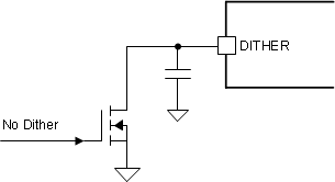
Connecting DITHER to AGND deactivates clock dithering, and the internal oscillator operates at a fixed frequency set by the RT resistor. Clock dithering is also disabled when an external synchronization pulse is applied.
 Figure 7-11 Dynamic Dither On/Off
Example