ZHCSEW6G may 2013 – november 2020 DS90UB913A-Q1
PRODUCTION DATA
- 1
- 1特性
- 2应用
- 3说明
- 4Revision History
- Device Comparison Table
- 5Pin Configuration and Functions
-
6Specifications
- 6.1 Absolute Maximum Ratings
- 6.2 ESD Ratings
- 6.3 Recommended Operating Conditions
- 6.4 Thermal Information
- 6.5 Electrical Characteristics
- 6.6 Recommended Serializer Timing For PCLK
- 6.7 AC Timing Specifications (SCL, SDA) - I2C-Compatible
- 6.8 Bidirectional Control Bus DC Timing Specifications (SCL, SDA) - I2C-Compatible
- 6.9 Timing Diagrams
- 6.10 Serializer Switching Characteristics
- 6.11 Typical Characteristics
- 7Detailed Description
- Application and Implementation
- Power Supply Recommendations
- 8Layout
- 9Device and Documentation Support
- Mechanical, Packaging, and Orderable Information
7.4.7 Sample BIST Sequence
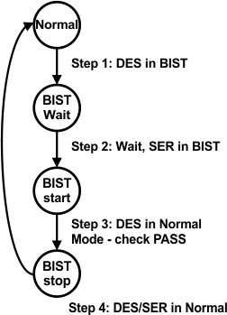
Step 1. For the DS90UB913A/914A FPD-Link III chipset, BIST Mode is enabled via the BISTEN pin of DS90UB914A-Q1 FPD-Link III deserializer. The desired clock source is selected through the deserializer GPIO0 and GPIO1 pins as shown in Table 7-4.
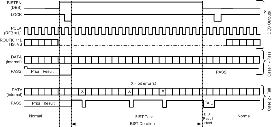
Step 2. The DS90UB913A-Q1 Serializer BIST pattern is enabled through the back channel. The BIST pattern is sent through the FPD-Link III to the deserializer. Once the serializer and deserializer are in the BIST mode and the deserializer acquires Lock, the PASS pin of the deserializer goes high and BIST starts checking FPD-Link III serial stream. If an error in the payload is detected, the PASS pin will switch low for one half of the clock period. During the BIST test, the PASS output can be monitored and counted to determine the payload error rate.
Step 3. To stop the BIST mode, the deserializer BISTEN pin is set LOW. The deserializer stops checking the data. The final test result is not maintained on the PASS pin. To monitor the BIST status, check the BIST Error Count register, 0x25 on the Deserializer.
Step 4. The link returns to normal operation after the deserializer BISTEN pin is low. Figure 7-8 shows the waveform diagram of a typical BIST test for two cases. Case 1 is error free, and Case 2 shows one with multiple errors. In most cases, it is difficult to generate errors due to the robustness of the link (differential data transmission etc.), thus they may be introduced by greatly extending the cable length, faulting the interconnect, or by reducing signal condition enhancements (Rx equalization).
 Figure 7-7 AT-Speed BIST System Flow Diagram
 Figure 7-8 BIST Timing Diagram