ZHCSIS6B September 2018 – December 2018 ADS1278-SP
PRODUCTION DATA.
- 1 特性
- 2 应用
- 3 说明
- 4 修订历史记录
- 5 说明 (续)
- 6 Pin Configuration and Functions
- 7 Specifications
-
8 Detailed Description
- 8.1 Overview
- 8.2 Functional Block Diagram
- 8.3
Feature Description
- 8.3.1 Sampling Aperture Matching
- 8.3.2 Frequency Response
- 8.3.3 Phase Response
- 8.3.4 Settling Time
- 8.3.5 Data Format
- 8.3.6 Analog Inputs (AINP, AINN)
- 8.3.7 Voltage Reference Inputs (VREFP, VREFN)
- 8.3.8 Clock Input (CLK)
- 8.3.9 Mode Selection (MODE)
- 8.3.10 Synchronization (SYNC)
- 8.3.11 Power-Down (PWDN)
- 8.3.12 Format[2:0]
- 8.3.13 Serial Interface Protocols
- 8.3.14 SPI Serial Interface
- 8.3.15 Frame-Sync Serial Interface
- 8.3.16 DOUT Modes
- 8.3.17 Daisy-Chaining
- 8.3.18 Modulator Output
- 8.3.19 Pin Test Using Test[1:0] Inputs
- 8.3.20 VCOM Output
- 8.4 Device Functional Modes
- 9 Application and Implementation
- 10Power Supply Recommendations
- 11Layout
- 12器件和文档支持
- 13机械、封装和可订购信息
8.3.7 Voltage Reference Inputs
(VREFP, VREFN)
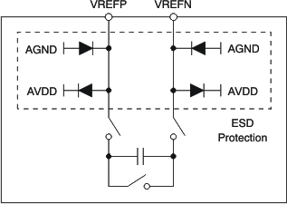
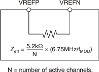
The voltage reference for the ADS1278-SP ADC is the differential voltage between VREFP and VREFN: VREF = (VREFP – VREFN). The voltage reference is common to all channels. The reference inputs use a structure similar to that of the analog inputs with the equivalent circuitry on the reference inputs shown in Figure 66. As with the analog inputs, the load presented by the switched capacitor can be modeled with an effective impedance, as shown in Figure 67. However, the reference input impedance depends on the number of active (enabled) channels in addition to fMOD. As a result of the change of reference input impedance caused by enabling and disabling channels, the regulation and setting time of the external reference should be noted, so as not to affect the readings.
 Figure 66. Equivalent Reference Input Circuitry
  Figure 67. Effective Reference Impedance
 ESD diodes protect the reference inputs. To keep these diodes from turning on, make sure the voltages on the reference pins do not go below AGND by more than 0.4 V, and likewise do not exceed AVDD by 0.4 V. If these conditions are possible, external Schottky clamp diodes or series resistors may be required to limit the input current to safe values (see the Absolute Maximum Ratings table).
Note that the valid operating range of the reference inputs is limited to the following parameters:
–0.1 V ≤ VREFN ≤ +0.1 V
VREFN + 0.5 V ≤ VREFP ≤ AVDD + 0.1 V