ZHCSIS6B September 2018 – December 2018 ADS1278-SP
PRODUCTION DATA.
- 1 特性
- 2 应用
- 3 说明
- 4 修订历史记录
- 5 说明 (续)
- 6 Pin Configuration and Functions
- 7 Specifications
-
8 Detailed Description
- 8.1 Overview
- 8.2 Functional Block Diagram
- 8.3
Feature Description
- 8.3.1 Sampling Aperture Matching
- 8.3.2 Frequency Response
- 8.3.3 Phase Response
- 8.3.4 Settling Time
- 8.3.5 Data Format
- 8.3.6 Analog Inputs (AINP, AINN)
- 8.3.7 Voltage Reference Inputs (VREFP, VREFN)
- 8.3.8 Clock Input (CLK)
- 8.3.9 Mode Selection (MODE)
- 8.3.10 Synchronization (SYNC)
- 8.3.11 Power-Down (PWDN)
- 8.3.12 Format[2:0]
- 8.3.13 Serial Interface Protocols
- 8.3.14 SPI Serial Interface
- 8.3.15 Frame-Sync Serial Interface
- 8.3.16 DOUT Modes
- 8.3.17 Daisy-Chaining
- 8.3.18 Modulator Output
- 8.3.19 Pin Test Using Test[1:0] Inputs
- 8.3.20 VCOM Output
- 8.4 Device Functional Modes
- 9 Application and Implementation
- 10Power Supply Recommendations
- 11Layout
- 12器件和文档支持
- 13机械、封装和可订购信息
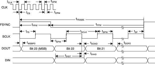
7.7 Timing Requirements: Frame-Sync Format(4)
over operating free-air temperature range (unless otherwise noted)| SYMBOL | PARAMETER | MIN | TYP | MAX | UNIT | |
|---|---|---|---|---|---|---|
| tCLK | CLK period (1 / fCLK) | All modes | 37 | 10,000 | ns | |
| High-Speed mode only | 30.5 | ns | ||||
| tCPW | CLK positive or negative pulse width | 12 | ns | |||
| tCS | Falling edge of CLK to falling edge of SCLK | –0.25 | 0.25 | tCLK | ||
| tFRAME | Frame period (1 / fDATA)(1) | 256 | 2560 | tCLK | ||
| tFPW | FSYNC positive or negative pulse width | 1 | tSCLK | |||
| tFS | Rising edge of FSYNC to rising edge of SCLK | 5 | ns | |||
| tSF | Rising edge of SCLK to rising edge of FSYNC | 5 | ns | |||
| tSCLK | SCLK period(2) | 1 | tCLK | |||
| tSPW | SCLK positive or negative pulse width | 0.4 | tCLK | |||
| tDOHD(5)(3) | SCLK falling edge to old DOUT invalid (hold time) | 10 | ns | |||
| tDOPD(3) | SCLK falling edge to new DOUT valid (propagation delay) | 31 | ns | |||
| tMSBPD | FSYNC rising edge to DOUT MSB valid (propagation delay) | 31 | ns | |||
| tDIST | New DIN valid to falling edge of SCLK (setup time) | 6 | ns | |||
| tDIHD(5) | Old DIN valid to falling edge of SCLK (hold time) | 6 | ns | |||
(1) Depends on MODE[1:0] and CLKDIV selection. See Table 5 (fCLK / fDATA).
(2) SCLK must be continuously running and limited to ratios of 1, 1/2, 1/4, and 1/8 of fCLK.
(3) Load on DOUT = 20 pF.
(4) Timing parameters are characterized or assured by design for specified temperature but not production tested.
(5) tDOHD (DOUT hold time) and tDIHD (DIN hold time) are specified under opposite worst-case conditions (digital supply voltage and ambient temperature). Under equal conditions, with DOUT connected directly to DIN, the timing margin is > 4 ns.
 Figure 2. Frame-Sync Format Timing Characteristics