ZHCSIS6B September 2018 – December 2018 ADS1278-SP
PRODUCTION DATA.
- 1 特性
- 2 应用
- 3 说明
- 4 修订历史记录
- 5 说明 (续)
- 6 Pin Configuration and Functions
- 7 Specifications
-
8 Detailed Description
- 8.1 Overview
- 8.2 Functional Block Diagram
- 8.3
Feature Description
- 8.3.1 Sampling Aperture Matching
- 8.3.2 Frequency Response
- 8.3.3 Phase Response
- 8.3.4 Settling Time
- 8.3.5 Data Format
- 8.3.6 Analog Inputs (AINP, AINN)
- 8.3.7 Voltage Reference Inputs (VREFP, VREFN)
- 8.3.8 Clock Input (CLK)
- 8.3.9 Mode Selection (MODE)
- 8.3.10 Synchronization (SYNC)
- 8.3.11 Power-Down (PWDN)
- 8.3.12 Format[2:0]
- 8.3.13 Serial Interface Protocols
- 8.3.14 SPI Serial Interface
- 8.3.15 Frame-Sync Serial Interface
- 8.3.16 DOUT Modes
- 8.3.17 Daisy-Chaining
- 8.3.18 Modulator Output
- 8.3.19 Pin Test Using Test[1:0] Inputs
- 8.3.20 VCOM Output
- 8.4 Device Functional Modes
- 9 Application and Implementation
- 10Power Supply Recommendations
- 11Layout
- 12器件和文档支持
- 13机械、封装和可订购信息
8.3.6 Analog Inputs (AINP, AINN)
The ADS1278-SP measures each differential input signal VIN = (AINP – AINN) against the common differential reference VREF = (VREFP – VREFN). The most positive measurable differential input is +VREF, which produces the most positive digital output code of 7FFFFFh. Likewise, the most negative measurable differential input is –VREF, which produces the most negative digital output code of 800000h.
For optimum performance, the inputs of the ADS1278-SP are intended to be driven differentially. For single-ended applications, one of the inputs (AINP or AINN) can be driven while the other input is fixed (typically to AGND or 2.5 V). Fixing the input to 2.5 V permits bipolar operation, thereby allowing full use of the entire converter range.
While the ADS1278-SP measures the differential input signal, the absolute input voltage is also important. This value is the voltage on either input (AINP or AINN) with respect to AGND. The range for this voltage is:
–0.1 V < (AINN or AINP) < AVDD + 0.1 V
If either input is taken below –0.4 V or above (AVDD + 0.4 V), ESD protection diodes on the inputs may turn on. If these conditions are possible, external Schottky clamp diodes or series resistors may be required to limit the input current to safe values (see the Absolute Maximum Ratings table).
The ADS1278-SP is a very high-performance ADC. For optimum performance, it is critical that the appropriate circuitry be used to drive the ADS1278-SP inputs. See the Application Information section for several recommended circuits.
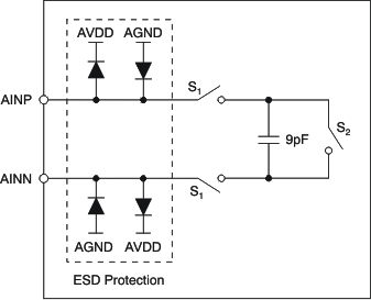
The ADS1278-SP uses switched-capacitor circuitry to measure the input voltage. Internal capacitors are charged by the inputs and then discharged. Figure 63 shows a conceptual diagram of these circuits. Switch S2 represents the net effect of the modulator circuitry in discharging the sampling capacitor; the actual implementation is different. The timing for switches S1 and S2 is shown in Figure 64. The sampling time (tSAMPLE) is the inverse of modulator sampling frequency (fMOD) and is a function of the mode, the CLKDIV input, and CLK frequency, as shown in Table 4.
 Figure 63. Equivalent Analog Input Circuitry
  Figure 64. S1 and S2 Switch Timing for Figure 63
 Table 4. Modulator Frequency (FMOD) Mode Selection
| MODE SELECTION | CLKDIV | fMOD |
|---|---|---|
| High-Speed | 1 | fCLK / 4 |
| High-Resolution | 1 | fCLK / 4 |
| Low-Power | 1 | fCLK / 8 |
| 0 | fCLK / 4 | |
| Low-Speed | 1 | fCLK / 40 |
| 0 | fCLK / 8 |
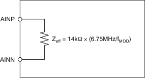
The average load presented by the switched capacitor input can be modeled with an effective differential impedance, as shown in Figure 65. Note that the effective impedance is a function of fMOD.
 Figure 65. Effective Input Impedances