ZHCSIS6B September 2018 – December 2018 ADS1278-SP
PRODUCTION DATA.
- 1 特性
- 2 应用
- 3 说明
- 4 修订历史记录
- 5 说明 (续)
- 6 Pin Configuration and Functions
- 7 Specifications
-
8 Detailed Description
- 8.1 Overview
- 8.2 Functional Block Diagram
- 8.3
Feature Description
- 8.3.1 Sampling Aperture Matching
- 8.3.2 Frequency Response
- 8.3.3 Phase Response
- 8.3.4 Settling Time
- 8.3.5 Data Format
- 8.3.6 Analog Inputs (AINP, AINN)
- 8.3.7 Voltage Reference Inputs (VREFP, VREFN)
- 8.3.8 Clock Input (CLK)
- 8.3.9 Mode Selection (MODE)
- 8.3.10 Synchronization (SYNC)
- 8.3.11 Power-Down (PWDN)
- 8.3.12 Format[2:0]
- 8.3.13 Serial Interface Protocols
- 8.3.14 SPI Serial Interface
- 8.3.15 Frame-Sync Serial Interface
- 8.3.16 DOUT Modes
- 8.3.17 Daisy-Chaining
- 8.3.18 Modulator Output
- 8.3.19 Pin Test Using Test[1:0] Inputs
- 8.3.20 VCOM Output
- 8.4 Device Functional Modes
- 9 Application and Implementation
- 10Power Supply Recommendations
- 11Layout
- 12器件和文档支持
- 13机械、封装和可订购信息
8.3.4 Settling Time
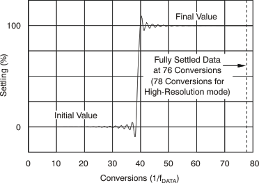
As with frequency and phase response, the digital filter also determines settling time. Figure 62 shows the output settling behavior after a step change on the analog inputs normalized to conversion periods. The X-axis is given in units of conversion. Note that after the step change on the input occurs, the output data change very little prior to 30 conversion periods. The output data are fully settled after 76 conversion periods for High-Speed and Low-Power modes, and 78 conversion periods for High-Resolution mode.
 Figure 62. Step Response