ZHCSGX4C June 2017 – April 2021 BQ40Z50-R2
PRODUCTION DATA
- 1 特性
- 2 应用
- 3 说明
- 4 Revision History
- 5 Description (continued)
- 6 Pin Configuration and Functions
-
7 Specifications
- 7.1 Absolute Maximum Ratings
- 7.2 ESD Ratings
- 7.3 Recommended Operating Conditions
- 7.4 Thermal Information
- 7.5 Supply Current
- 7.6 Power Supply Control
- 7.7 AFE Power-On Reset
- 7.8 AFE Watchdog Reset and Wake Timer
- 7.9 Current Wake Comparator
- 7.10 VC1, VC2, VC3, VC4, BAT, PACK
- 7.11 SMBD, SMBC
- 7.12 PRES, BTP_INT, DISP
- 7.13 LEDCNTLA, LEDCNTLB, LEDCNTLC
- 7.14 Coulomb Counter
- 7.15 CC Digital Filter
- 7.16 ADC
- 7.17 ADC Digital Filter
- 7.18 CHG, DSG FET Drive
- 7.19 PCHG FET Drive
- 7.20 FUSE Drive
- 7.21 Internal Temperature Sensor
- 7.22 TS1, TS2, TS3, TS4
- 7.23 PTC, PTCEN
- 7.24 Internal 1.8-V LDO
- 7.25 High-Frequency Oscillator
- 7.26 Low-Frequency Oscillator
- 7.27 Voltage Reference 1
- 7.28 Voltage Reference 2
- 7.29 Instruction Flash
- 7.30 Data Flash
- 7.31 OLD, SCC, SCD1, SCD2 Current Protection Thresholds
- 7.32 Timing Requirements: OLD, SCC, SCD1, SCD2 Current Protection Timing
- 7.33 Timing Requirements: SMBus
- 7.34 Timing Requirements: SMBus XL
- 7.35 Typical Characteristics
-
8 Detailed Description
- 8.1 Overview
- 8.2 Functional Block Diagram
- 8.3
Feature Description
- 8.3.1 Primary (1st Level) Safety Features
- 8.3.2 Secondary (2nd Level) Safety Features
- 8.3.3 Charge Control Features
- 8.3.4 Gas Gauging
- 8.3.5 Configuration
- 8.3.6 Battery Parameter Measurements
- 8.3.7 Battery Trip Point (BTP)
- 8.3.8 Lifetime Data Logging Features
- 8.3.9 Authentication
- 8.3.10 LED Display
- 8.3.11 IATA Support
- 8.3.12 Voltage
- 8.3.13 Current
- 8.3.14 Temperature
- 8.3.15 Communications
- 8.4 Device Functional Modes
- 9 Application and Implementation
- 10Power Supply Recommendations
- 11Layout
- 12Device and Documentation Support
- 13Mechanical, Packaging, and Orderable Information
9.2.2.3.3 PACK and FET Control
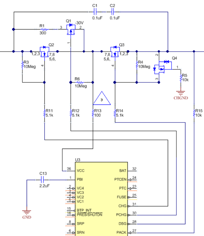
The PACK and VCC inputs provide power to the BQ40Z50-R2 device from the charger. The PACK input also provides a method to measure and detect the presence of a charger. The PACK input uses a 10-kΩ resistor; whereas, the VCC input uses an internal diode to guard against input transients and prevent a misoperation of the gate driver during short-circuit events.
 Figure 9-13 BQ40Z50-R2 PACK and FET Control
The N-channel charge and discharge FETs are controlled with 5.1-kΩ series gate resistors, which provide a switching time constant of a few microseconds. The 10-MΩ resistors ensure that the FETs are off in the event of an open connection to the FET drivers. Q4 is provided to protect the discharge FET (Q3) in the event of a reverse-connected charger. Without Q4, Q3 can be driven into its linear region and suffer severe damage if the PACK+ input becomes slightly negative.
Q4 turns on in that case to protect Q3 by shorting its gate to source. To use the simple ground gate circuit, the FET must have a low gate turn-on threshold. If it is desired to use a more standard device, such as the 2N7002 as the reference schematic, the gate should be biased up to 3.3 V with a high-value resistor. The BQ40Z50-R2 device has the capability to provide a current-limited charging path typically used for low battery voltage or low temperature charging. The BQ40Z50-R2 device uses an external P-channel, precharge FET controlled by PCHG.